Boost Converter Design
The Design of Boost DC to DC Converters
Before reading this section, please read the Introduction to DC to DC Converter Design.
All of the circuits in this tutorial can be simulated in LTspice®. If you are new to LTspice, please have a look at my LTspice Tutorial
Consider the architecture of a boost converter, shown in Figure 1.
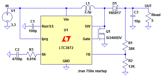
Figure 1
The MOSFET, Q1, switches on creating a short circuit between the right hand side of the inductor, L1, and 0V. Thus a fixed voltage of 3.3V is applied across the inductor, so its current will ramp up according to
or
or 1.5 million amps per second. Thus if the MOSFET switches off after 1us, the current through the inductor will have ramped up by 1.5A.
When the MOSFET switches off, the inductor tries to maintain its current flow. It does this by generating a voltage across its terminals very similar to a battery, where the current flows from the negative terminal, through the battery, to the positive terminal.
In the circuit of Figure 1, we can see that to maintain current flow, the right hand side of the inductor has to increase in voltage with respect to the left hand side. The left hand side is connected to the input voltage (so cannot change), thus the right hand side voltage increases above the input voltage and continues to do so until something conducts. Theoretically, this voltage will rise to an infinite value, making the inductor very good at generating high voltages from low voltages.
In Figure 1, the inductor voltage increases until diode D1 conducts after which the energy in the inductor flows into the output capacitor C3, causing the voltage across C3 to increase slightly. It is worth noting that even before the MOSFET has started to switch, there is a dc path flowing from the input, through L1 and diode D1 into C3, so at startup C3 will have a voltage across it (equal to Vin – Vdiode).
When the MOSFET switches off and the inductor discharges, the inductor still behaves according to
except this time, the voltage across the inductor is equal to Vout – Vin (ignoring the diode drop).
When the inductor has discharged, the MOSFET switches on and the process starts again. Repeating this process produces pulses of energy from the inductor into the output capacitor making the voltage across the output capacitor rise. In Figure1, resistors R1 and R2 monitor the output voltage and when the voltage at the FB pin reaches a certain point, the chip terminates the drive to the MOSFET until the voltage on the output capacitor droops.
The LTspice model of this circuit can be downloaded here (right click over the link and save as a '.asc' file). LTC3872 Boost Converter
The LTspice simulation results are shown in Figure 2. Here we are looking at the part operating once the output voltage has ramped up to 5V.
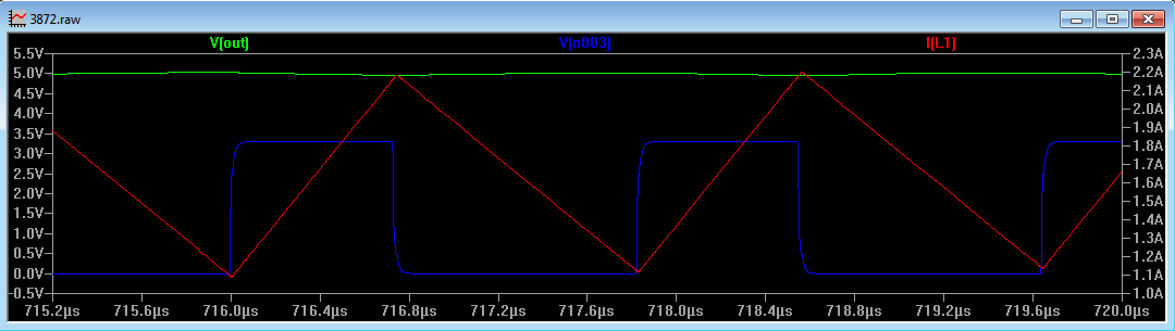
Figure 2
The blue waveform is the Gate voltage to the MOSFET. When the FET turns on, the inductor current (in red) ramps up from 1.09A to 2.18A in 739ns (this can be measured in LTspice), or at a rate of 1.474 million Amps per second, close to what we calculated above. The discrepancy is due to the fact that the FET does not provide a true short circuit to ground and actually has a voltage across it of approximately 50mV when switched on, thus reducing the voltage across the inductor.
Likewise when the FET switches off, the current ramps from 2.18A to 1.09A in 1.083us. From the equation
Likewise when the FET switches off, the current ramps from 2.18A to 1.09A in 1.083us. From the equation
once the output has reached regulation the voltage across the inductor is [(5+Vd) - 3.3], where Vd is the voltage across the diode (approx. 0.5V), so we can calculate the current ramp to be
or 1 million amps per second. Over a period of 1.083us, the current ramps down by 1.083A, so again our LTspice simulation is very close to the calculated value.
It is useful to calculate the duty cycle (the ratio of the ON time of the FET to the total period of oscillation).
Again from the equation
we can see that during ramp up, the inductor current di is represented by
where dt1 is the ON time of the FET and Vin is the input voltage.
During ramp down, the inductor current is represented by
where Vout is the output voltage and dt2 is the OFF time of the FET. To make life easier, we have neglected the diode voltage drop.
For a fixed input voltage and a fixed output voltage, di is the same when ramping up as ramping down.
Thus, equating di gives
From this we can calculate
Now, our duty cycle, DC is represented by
Hence
So
So from there we can work out that
The duty cycle is set by the input and output voltages only. The inductor value does not feature in setting the duty cycle, nor does the controller IC.
The above is true as long as the current in the inductor does not fall to zero. This is called Continuous Conduction Mode (CCM). If the inductor current falls to zero, the duty cycle equation above does not hold and the controller enters Discontinuous Conduction Mode (DCM).
In CCM, if the load current increases, the duty cycle remains unchanged (in steady state). The circuit reacts to the increase in load current by keeping the duty cycle constant, but the midpoint of the inductor current (its dc offset) increases. The switching frequency and the amplitude of the inductor ripple current remain unchanged. In FIG 2, the midpoint of the inductor current is approximately 1.65A and the ripple amplitude is 1.1A. If the load increases the midpoint of the current will increase, but the inductor ripple current will still be 1.1A.
In a boost converter, the average input current is equal to the average inductor current. The circuit of FIG 1 produces a 5V output into 5 Ohms (1A), so we have a 5W load. If we assume the efficiency of the converter is 90%, this means we need an input power of
With an input voltage of 3.3V, this implies a current of 1.68A. We can see from FIG 2 that the average input current is roughly 1.68A.
Boost Converter Design Procedure
Below is a worked example using the theory outlined above. It is based on the general purpose boost converter, the LT3757 (LT3757 datasheet).
Our brief is to design a boost converter that converts 5V to 12V and supplies a load of 1A. The output ripple should be less than 2%. The switching frequency needs to be approx. 500kHz. This switching frequency might be imposed on us to ensure that the dc/dc converter is not operating at the same frequency as other sensitive electronics in the circuit. Also, generally a faster switching frequency leads to a smaller inductor size, but the switching losses in the circuit increase, so 500kHz is normally a sweet spot to ensure good efficiency, but small components.
Inductor Choice
With a 12V/1A output, this represents a load of 12W. Page 1 of the datasheet shows that our efficiency is going to be about 90%, implying that our input power is:
With a 5V input, this represents an average input current of
The optimal ripple current of the inductor is 40% of the output current. This is a good rule of thumb for most dc/dc converters and represents a trade off between small inductor size and low switching losses.
Our inductor current is 2.67A, so for 40% ripple the peak current needs to be (2.67 x 1.2 = 3.2A). Our minimum inductor current needs to be (2.67 x 0.8 = 2.14A). This gives a change in current of (3.2 – 2.14 = 1.06A).
We know our duty cycle is represented by
which is
A switching frequency of 500kHz has a period of 2us, so the MOSFET switches on for
(at this point, it is worth checking the controller’s minimum ON time to see if we are comfortably within the specification. The LT3757 has a minimum ON time of 220ns, so we are OK).
We have calculated that our current needs to change by 1.06A, so our change in current with time is
When the MOSFET is on, the voltage across the inductor is equal to our input voltage (5V), so from this we can work out the inductor value from
So our inductor value calculates to be 5.47uH.
Now, if too much current flows in the inductor, the ferrite that it is wound on saturates with the effect that its inductance rapidly decreases. From the equation above, if the inductance decreases the change in current with time increases, worsening the effect of the over current, so we must ensure that the inductor we choose is rated to handle the current. Thus the saturation rating of the inductor needs to be in excess of the peak current of 3.2A. A saturation rating of 3.5A should suffice.
Wurth Electronics have 2 suitable solutions (which can be found using the Wurth Electronics Component Simulation Software):
There is little difference in either of these components, so the 4.7uH will be chosen as this is closer.
Rsense Calculation
The sense resistor feeds into the PWM engine inside the controller as well as determining the maximum current that can flow through the inductor. The inductor current flows through the sense resistor, creating a ramp voltage across it. If this voltage exceeds 100mV (see the datasheet), the MOSFET is switched off to protect the surrounding circuitry from over current.
We have calculated above that our peak inductor current is 3.2A, so our sense resistor has to be selected such that this current does not exceed the sense threshold of 100mV (worst case spec).
To allow a 20% margin, let’s assume that the current sense trip threshold is 80mV. For a peak current of 3.2A, this means a sense resistor value of 25mOhms. Putting this back into the datasheet specification of 100mV, this means our worst case inductor current will be 4A, well below the 5.5A rating of our inductor.
MOSFET Choice
The MOSFET needs to be able to handle the peak inductor current so in this design a drain source current rating (Id) of 10A is more than sufficient. The Drain–Source voltage (Vds) needs to be in excess of the output voltage + diode drop, so anything above 20V is suitable for a 12V output.
The Gate-Source turn on voltage of the MOSFET (Vgs) needs to be less than the input voltage, to ensure that the voltage coming out of the Gate pin can actually activate the MOSFET. Logic level MOSFETs have a low turn on voltage, are widely available and usually perfect for low voltage dc/dc converters.
The above parameters represent the bare minimum characteristics of the MOSFET. However, to get a good design, we must ensure that the losses in the MOSFET are as low as possible. The MOSFET switch presents 2 losses in the circuit: switching losses and conduction losses.
The switching losses result from current flowing through the MOSFET at the same time that a voltage is across the MOSFET (so power is generated in the MOSFET), during the turn on and turn off times of the MOSFET. For a given gate drive coming out of the controller IC, the lower the Gate-Source capacitance of the MOSFET, the quicker the MOSFET will turn on. Thus the Qg specification of the MOSFET is important and should be as low as possible. The Qg of the MOSFET will also have an impact on the heat dissipation of the chip, especially if the input voltage to the chip is high.
Charge is dictated by the equation:
Charge (Q) = Current (I) x Time (s)
Since Frequency is the inverse of Time, we can write
So we can calculate the current needed to flow into the chip, just to charge the gate capacitance of the FET. Since heat is the product of voltage and current, if the gate charge is high and/or the switching frequency is high, the heat dissipation in the chip will be high if the input voltage is high.
Once the MOSFET has switched on, the MOSFET presents a small dc resistance between its Drain and Source terminals. This is the MOSFETs ‘Drain Source on resistance’ or RDSon. Again, this needs to be as low as possible.
Now, MOSFET manufacturers reduce the ON resistance of the MOSFET by constructing many parallel conduction paths between the Drain and Source. Thus, like connecting resistors in parallel, the ON resistance comes down with more parallel paths. However, in connecting Drain Source paths in parallel, a negative effect is that the Gate Source capacitance (Qg) is also connected in parallel, so a low ON resistance (and hence low conduction loss) sometimes implies a high gate source capacitance (hence high switching loss). Thus the MOSFET that is chosen should be a compromise between these two characteristics. In addition, high current MOSFETs tend to come in much larger packages, so meeting the ideals of low ON resistance and low Qg might violate a space requirement spec, so the selection process has to start over. Engineering, as ever, is a compromise.
Indeed looking at the selection tables of the MOSFET manufacturers, it is better to select a MOSFET with a low ON resistance (less than 10mOhms), then filter this selection to remove MOSFETs with a Qg of greater than 10nC, then select a MOSFET from this list, as long as the Gate turn on voltage, Vds and Id can be met. Starting by selecting MOSFETs with a Vds of between 20V and 30V might rule out some higher voltage FETs that are better suited to lower voltage designs. Failing that, download all the results to a spreadsheet and sort from there. I have never had much luck with the parametric searches on MOSFET websites.
Alternatively, download all the MOSFET characteristics into a spreadsheet, remove the ones that don't meet the VDS and ID requirements, then add a column called FOM (Figure of Merit). This column should contain the value RDSON x QG. Then sort by this column and pick the FET with the lowest FOM. This part will be the best compromise between RDSON and QG and ideal for the top MOSFET.
If the ideal of low ON resistance and low Qg cannot be met, look at the duty cycle. If the output voltage is not much higher than the input voltage then the duty cycle will be low, so the ON time of the FET will be small as a proportion of the total switching period. Therefore low Qg is of more importance and low ON resistance is of less importance. Likewise, a high output voltage implies a high duty cycle hence low ON resistance is of more importance then low Qg.
The Fairchild FDS6680 represents a good compromise between low ON resistance and low gate charge, but its SO8 package is large and therefore might be unsuitable for compact designs.
Rectifier Diode Choice
When the MOSFET switches off, the inductor voltage ramps rapidly in order to maintain current flow. Many diodes are not fast enough to react to this voltage change, resulting in a large spike on the Drain of the MOSFET. This can (and does) destroy the MOSFET.
Therefore Schottky diodes should be used in all dc/dc converter designs where the inductor voltage has to be rectified. Ultra fast diode have a response time of 10’s of nanoseconds, standard rectifier diodes have a response time of several microseconds, whereas a Schottky has a response time in the order of a few nanoseconds. Schottky diodes also have a much lower forward voltage drop (0.3V) compared with standard rectifiers (0.6V) so half the power is wasted as a result of VxI losses.
When choosing a Schottky diode, the key parameters are: forward voltage drop (should be as low as possible), forward current (this should be greater than the peak inductor current) and reverse voltage rating. When the FET is charging the inductor, the anode of the Schottky diode will be at 0V and the cathode will be at Vout, so the reverse voltage rating of the Schottky should be greater than Vout.
In this design example, the MBRS340 is a good choice with a reverse voltage rating of 40V and a forward voltage of 0.53V at 3A peak current.
Output Capacitor Choice
Unlike the buck converter that has a continuous current flowing from the inductor into the output capacitor, the boost converter output capacitor has to keep the output voltage alive when the inductor is being charged (and is hence disconnected from the output). Therefore there will be a component of the output ripple due to the discharge of the output capacitor.
In addition, when the inductor is discharging, the output capacitor will experience an inrush of current and any ESR (effective series resistance) in the capacitor will also result in ripple.
Therefore the output ripple is made up of 2 components: the ripple caused by the output capacitor discharging when the inductor is being charged and the ripple caused by the inrush current from the inductor into the ESR of the output capacitor. The design spec states that the output ripple needs to be less than 2%. For the following calculations, it is assumed that 1% of the output ripple is discharge ripple and 1% is ESR ripple.
The ripple caused by the discharge of the output capacitor while the inductor is charging is dictated by
where i is the load current in Amps, C is the output capacitance in Farads and dv/dt is the change in output voltage with time.
Earlier we calculated that the MOSFET switches on for a period of 1.16us. If we require a discharge ripple of 1% (120mV) with a load current of 1A, this implies we need a capacitance of
or 9.66uF.
Note that when the inductor is charging, there is zero current flowing in the rectifier diode. When the MOSFET switches off, the diode current jumps from 0A to the peak inductor current, so it is the peak inductor current, not the ripple current amplitude that determines this component of the output ripple (compare this with the ripple in a buck converter that is determined by the ripple current amplitude, not the peak inductor current).
The ripple caused by the ESR is a product of the peak inductor current and the ESR. In our example the peak current is 3.2A. The ESR is of a typical tantalum capacitor is about 70m Ohms, giving a ripple of 224mV. Two capacitors in parallel halve the ESR but double the capacitance, so yield an effective ESR of 35m Ohms and an ESR ripple of 112mV.
Ceramic capacitors have a much lower ESR (approx. 10m Ohm), so the ESR ripple is significantly reduced if ceramic output capacitors are used.
Therefore two 6.8uF tantalum capacitors, each with an ESR of 70m Ohm will give an ESR ripple of 112mV and a discharge ripple of 85mV. The total ripple is thus 197mV which is less than the 2% ripple of the design spec.
Other points to note
The feedback resistor values can be calculated using the Feedback Resistor Calculator:
The feedback resistors were picked as 11k and 71.5k so that a 12V output keeps the feedback point at 1.6V. Some engineers make these resistor values way too big in the hope of conserving wasted current in the feedback loop. However, this can have a negative effect in that too high resistor values (over 500k Ohms) can cause a phase shift created by the internal capacitance of the feedback pin and the large external resistor values which will lead to poor stability. In lower power designs (where feedback current is important), bypassing the top feedback resistor with 100pF overcomes this issue by providing a phase lead that counteracts the phase lag created by the input capacitance.
Please refer to the datasheet for information on how to set the Under Voltage Lockout (UVLO) and switching frequency.
The final LTspice circuit is shown in Figure 3
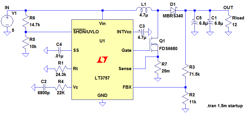
Figure 3
The LTspice circuit can be downloaded here (right click over the link and save as a '.asc' file): LT3757 Boost Converter
This text has explained the basics of boost converter switched mode power supply design and is applicable to most boost converters. Refer to the individual datasheets for a complete guide to designing with that particular part.
LTspice is a registered trademark of Analog Devices Inc
This text has explained the basics of boost converter switched mode power supply design and is applicable to most boost converters. Refer to the individual datasheets for a complete guide to designing with that particular part.
LTspice is a registered trademark of Analog Devices Inc
Sitemap: www.simonbramble.co.uk/sitemap
© Copyright Simon Bramble