Inverting Converter Design
The Design of Inverting DC to DC Converters
Before reading this page, please read the introduction.
All of the circuits in this tutorial can be simulated in LTspice®. If you are new to LTspice, please have a look at my LTspice Tutorial
Introduction
There are several ways of generating a negative voltage from a positive one, each with its own merits and drawbacks. This article will discuss the two popular architectures: the single inductor inverter and the Cuk (pronounced Chook) Converter (named after its inventor, Dr. Slobodan Ćuk).
As with all dc/dc converters, each one relies on the flyback properties of an inductor to generate the negative voltage.
(The Cuk converter is a superior solution to the single inductor inverter, but requires 2 inductors which is not desirable in some cases. As the two circuits have different ways of operating, each converter is described in detail, right from the basics, which makes this page rather long. If you want to skip to the Cuk converter, please scroll down and start reading from there)
Simple Inverter
A simple, single inductor based inverter is shown in Figure 1. This circuit converts a 5V input to -5V.
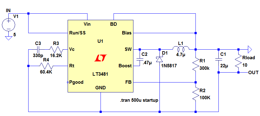
Figure 1
The LTspice circuit of Figure 1 can be downloaded here: Simple Inverting dc/dc converter.
The datasheet of the LT3481 can be downloaded here: LT3481 datasheet.
An internal transistor switches ON connecting Vin to SW, thus applying the input voltage across the inductor L1. The current ramps through the inductor according to the equation
The datasheet of the LT3481 can be downloaded here: LT3481 datasheet.
An internal transistor switches ON connecting Vin to SW, thus applying the input voltage across the inductor L1. The current ramps through the inductor according to the equation
where Vin is the input voltage (and the voltage across the inductor), L is the inductance value in Henries and di/dt is the change in current with time, measured in Amps per second. In the circuit in Figure 1, the above equation becomes
or 1.063 million amps per second. If the internal switch switches off after 1us, the current will have ramped up by 1.063A.
The LTspice simulation shows this current is 1.02 million amps per second. The slight error is due to the voltage drop across the switch causing a voltage slightly less than Vin being applied to the inductor.
When the transistor switches OFF, the inductor tries to maintain its current flow. It does this by generating a voltage across its terminals very similar to a battery, where the current flows from the negative terminal, through the battery, to the positive terminal. Since the right hand side of the inductor is clamped to 0V, the left hand side of the inductor flies negative. The Schottky diode, D1, conducts and clamps the left hand side of the inductor to about 0.3V below Vout and a current circulates clockwise down through the capacitor, up the diode and from left to right through the inductor, thus charging the capacitor. Since the upper terminal of the capacitor is at 0V, the lower terminal charges negatively and a negative voltage appears at the OUT terminal. The internal switch then switches ON again and the process starts over.
The inductor discharges according to the equation
(ignoring the diode drop).
Thus during discharge the change in current with time is also 1.063 million amps per second and this can be seen in LTspice.
The voltage across capacitor C1 is monitored by resistors R1 and R2 and when the junction of R1 and R2 reaches 1.265V (see LT3481 datasheet), the switching stops. Thus by setting R1 and R2 we can determine the final (negative) output voltage at OUT.
It is worth noting that the circuit in Figure 1 is very similar to a buck converter. Indeed the LT3481 is advertised as a buck converter and not an inverter. The only difference is that the node that was the output in the buck converter is now shorted to ground and the node that was 0V (including the ground pin of the controller) is now the negative output. Thus the ground pin of the LT3481 moves down in voltage as the capacitor charges, but the input voltage ground and the output voltage ground are the same node, so it is OK to short them together without things going bang. The input voltage is still referenced to 0V though.
A standard buck converter can be used as an inverter because the phasing of the feedback pin does not change. As the output capacitor charges negatively, the ground reference of the controller (the ground pin) is pulled negative, thus the voltage on all the other pins rise with respect to the ground pin. Thus the junction of R1 and R2 rises as the output capacitor charges – the same as a buck converter.
Compare this with the circuit of Figure 2. This is an alternative solution to the single inductor inverting dc/dc converter. Architecturally this is nearly identical to the circuit in Figure 1.
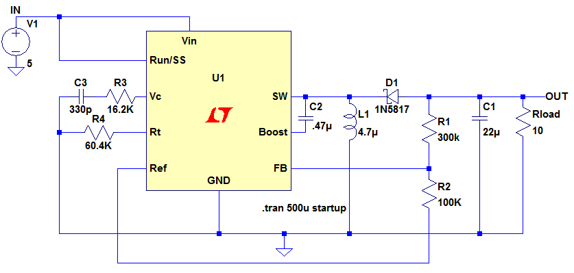
Figure 2
The input voltage is applied one end of the inductor (with the other end at ground) and the diode conducts on the inductor discharge cycle so the voltage at the OUT pin ramps to a negative voltage. Even the input and output share the same ground. However, here the feedback resistors, R1 and R2, are referenced to the REF pin (which is usually a positive voltage of approximately 1.2V). With 0V on the output, the junction of R1 and R2 is at a positive voltage and ramps negatively (so a standard buck converter cannot be used) as the OUT pin ramps to a negative voltage. R1 and R2 are scaled such that the junction of the resistors is at 0V when the output voltage reaches regulation.
The disadvantage of this architecture is that the REF pin has to source current into the feedback network and this might affect its accuracy, hence the accuracy of the output voltage. The accuracy of the output voltage is also dependent on the accuracy of the feedback resistors. The accuracy of the circuit in Figure 1 is only dependent on the accuracy of the feedback resistors. However, with the circuit in Figure 1, the controller is exposed to a supply voltage equal to the input voltage plus the magnitude of the output voltage, which can be quite high, but this is not normally a problem.
The input current (in green) and inductor current (in blue) for the circuit in Figure 3 are shown below.
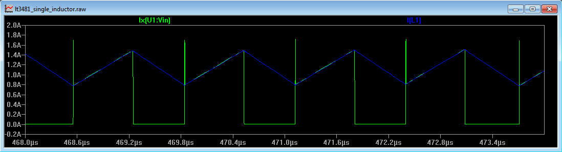
Figure 3
It is useful to determine the duty cycle of the converter. This is the ratio of the ON time of the switch to the total switching period.
The inductor charges according to
The inductor charges according to
and discharges according to
(ignoring the diode drop). We are also considering the magnitude of Vout to make the equations easier.
Thus, if the change in charge current is equal to the change in discharge current then
so
where dt1 is the charge time and dt2 is the discharge time of the inductor.
If we define the total switching period (dt1+dt2) as T then the duty cycle (DC) is
Therefore
so
becomes
and from here it can be found that
where Vout is the magnitude of Vout.
The duty cycle is set by the input and output voltages only. The inductor value does not feature in setting the duty cycle, nor does the controller IC. This is true as long as the current in the inductor does not fall to zero. This is called Continuous Conduction Mode (CCM). If the inductor current falls to zero, the duty cycle equation above does not hold and the controller enters Discontinuous Conduction Mode (DCM).
In CCM, if the load current increases, the duty cycle remains unchanged (in steady state). The circuit reacts to the increase in load current by keeping the duty cycle constant, but the midpoint of the inductor current (its dc offset) increases. The switching frequency and the amplitude of the inductor ripple current remain unchanged. In Figure 3, the midpoint of the inductor current is approximately 1.1A and the ripple amplitude is 700mA. If the load increases the midpoint of the current will increase, but the inductor ripple current will still be 700mA and the duty cycle will remain unchanged.
Now, the LT3481 is a buck converter and we have already stated that the circuit in Figure 1 is similar to that of a buck converter. Indeed it has the inductor/diode/capacitor configuration of a buck converter. With a buck converter the average inductor current (equal to the mid point of the inductor current) is also equal to the output current. Since Figure 1 is so similar to a buck converter, it would be convenient to assume that the average inductor current is also equal to the output current for the inverting configuration. However Figure 3 shows the average inductor current as approximately 1.1A when we know that the output current of Figure 1 is 500mA. The inverting configuration has a higher average inductor current because the inductor is actually disconnected from the output while it is charging. Consider a buck converter architecture shown in Figure 4. During the inductor charge phase, current flows through Q1, through the inductor and into the output capacitor. During the discharge phase, current flows up through Q2, through the inductor and into the output capacitor. On both the charge and discharge phase, the capacitor is always receiving current.
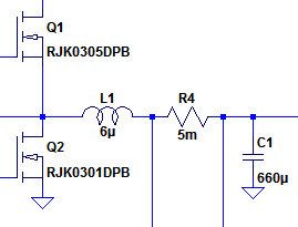
Figure 4
With the inverting configuration, shown in Figure 5, on the inductor charge phase, the current flows out of the SW pin through the inductor and down to ground. The output only receives current during the discharge phase. The shorter the duty cycle, the more time the discharge cycle can dump current into the load. Therefore, the average current in the inductor can be represented by
With a load current of 500mA (in Figure 1), and a duty cycle of 50%, the average inductor current will be 1A (assuming no losses).
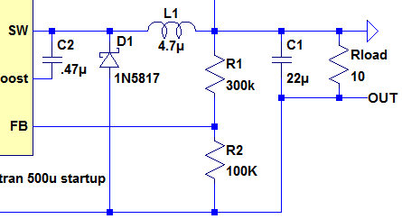
Figure 5
The single inductor inverter is simple, but due to the higher inductor current and sharp changes in current (see the green waveform in Figure 3), it does not present an elegant way of generating a negative voltage. A more suitable solution (the Cuk converter) will be discussed later.
For completion, below is a design example of a single inductor inverter.
Single Inductor Inverter Design Procedure
Our design brief is to design an inverting controller to convert 12V to -5V at 1A with a switching frequency of 400kHz.
An outline schematic is shown in Figure 6.
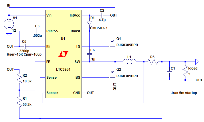
Figure 6
The LTC3854 is a standard buck converter, but in Figure 6 is wired as an inverter to give -5V/1A at the OUT terminal.
Inductor Choice
With an input voltage of 12V and an output voltage of -5V, the duty cycle is represented by
Inductor Choice
With an input voltage of 12V and an output voltage of -5V, the duty cycle is represented by
The LTC3854 switches at a frequency of 400kHz, so the ON time of the top MOSFET is 29% of 2.5us, or 725ns. A check of the datasheet shows that the minimum ON time of the LTC3854 is 75ns, so we are well within spec.
From
the average inductor current is 1.41A
The optimal ripple current of the inductor is 40% of the output current. This is a good rule of thumb for most dc/dc converters and represents a trade off between small inductor size and low switching losses. Therefore our design should have an inductor ripple current of 0.56A.
From the equation
during the charge phase the voltage across the inductor is equal to the input voltage, the value of di is 0.56A as calculated above and dt is 725ns. This means our ideal inductor value needs to be 15.53uH. With an average inductor current of 1.41A and a peak to peak inductor current of 0.56A, implies the peak current is 1.69A (and a trough current of 1.13A)
Now, if too much current flows in the inductor, the ferrite that it is wound on saturates with the effect that its inductance rapidly decreases. From the equation above, if the inductance decreases the change in current with time increases, worsening the effect of the over current, so we must ensure that the inductor we choose is rated to handle the current. Thus the saturation rating of the inductor needs to be in excess of the peak current of 1.69A. A saturation rating over 2A should suffice.
Wurth have a 15uH inductor with a saturation current rating of 2.2A
Rsense Calculation
As the inductor current ramps up it develops a voltage across the current sense resistor R3. The top MOSFET switches off when the voltage across the current sense resistor is 50mV (see LTC3854 datasheet). As stated above, the peak inductor current should be less than 2.2A, so a current sense resistor of 25mOhms ensures the peak current will be less than 2A.
MOSFET Choice - General
In nearly all applications the specification for the top MOSFET is different from that for the bottom MOSFET if maximum efficiency is to be achieved.
Both MOSFETs will be exposed to the difference between the input voltage and the output voltage at some point during the switching cycle, so must both have a drain-source breakdown voltage of at least (Vin + magnitude of Vout). In our design, the input voltage is 12V and the output voltage is -5V, so the minimum breakdown voltage should be 17V. A MOSFET rated with a breakdown voltage of at least 30V should suffice.
The peak current will occur just as the top MOSFET switches off and the bottom MOSFET switches on and the same magnitude of current flows through both devices. Our current sense resistor sets the peak current to 2A, so any MOSFET with a peak current greater than 5A is suitable.
Looking at the block diagram of the LTC3854, we see that the drive circuitry for the bottom MOSFET is powered from INTVCC. The minimum voltage specification on this voltage is 4.8V, so our bottom MOSFET must have a gate turn on voltage of significantly less than 4.8V.
However, the drive to the top MOSFET is powered from INTVCC – 0.3V (the voltage across the flying capacitor) so the turn on voltage of the top MOSFET needs to be significantly less than 4.5V.
In either case, a logic level MOSFET, with a turn on voltage of 1V - 2V is more suitable.
The above parameters represent the bare minimum characteristics of the MOSFETs. However, to get a good design, we must ensure that the losses in the MOSFETs are as low as possible.
MOSFET Choice – Switching and Conduction Losses
The MOSFET switches present 2 losses in the circuit: switching losses and conduction losses.
The switching losses result from current flowing through the MOSFET at the same time that a voltage is across the MOSFET (so power is generated in the MOSFET), during the turn on and turn off times of the MOSFET. For a given gate drive coming out of the controller IC, the lower the Gate-Source capacitance of the MOSFET, the quicker the MOSFET will turn on. Thus the Qg specification of the MOSFET is important and should be as low as possible. The Qg of the MOSFET will also have an impact on the heat dissipation of the IC, especially if the input voltage to the chip is high.
Charge is dictated by the equation:
Charge (Q) = Current (I) x Time (s)
Since Frequency is the inverse of Time, we can write
So we can calculate the current needed to flow into the chip, just to charge the gate capacitance of the FET. Since heat is the product of voltage and current, if the gate charge is high and/or the switching frequency is high, the heat dissipation in the chip will be high.
Once the MOSFET has switched on, the MOSFET presents a small dc resistance between its Drain and Source terminals. This is the MOSFETs ‘Drain Source ON resistance’ or RDSon. Again, this needs to be as low as possible.
Now, MOSFET manufacturers reduce the ON resistance of the MOSFET by constructing many parallel conduction paths between the Drain and Source. Thus, like connecting resistors in parallel, the ON resistance comes down with more parallel paths. However, in connecting Drain Source paths in parallel, a negative effect is that the Gate Source capacitance (Qg) is also connected in parallel, so a low ON resistance (and hence low conduction loss) sometimes implies a high gate source capacitance (hence high switching loss). Thus the MOSFET that is chosen should be a compromise between these two characteristics. In addition, high current MOSFETs tend to come in much larger packages, so meeting the ideals of low ON resistance and low Qg might violate a space requirement spec, so the selection process has to start over. Engineering, as ever, is a compromise.
Indeed looking at the selection tables of the MOSFET manufacturers, it is better to select a MOSFET with a low ON resistance (less than 10mOhms), then filter this selection to remove MOSFETs with a Qg of greater than 10nC, then select a MOSFET from this list, as long as the Gate turn on voltage, Vds and Id can be met. Starting by selecting MOSFETs with a Vds of between 20V and 30V might rule out some higher voltage FETs that are better suited to lower voltage designs. Failing that, download all the results to a spreadsheet and sort from there. I have never had much luck with the parametric searches on MOSFET websites.
Alternatively, download all the MOSFET characteristics into a spreadsheet, remove the ones that don't meet the VDS and ID requirements, then add a column called FOM (Figure of Merit). This column should contain the value RDSON x QG. Then sort by this column and pick the FET with the lowest FOM. This part will be the best compromise between RDSON and QG and ideal for the top MOSFET.
MOSFET Choice – Top MOSFET
The Duty Cycle governs how long the top MOSFET switches on for per period of the switching frequency. We have calculated that the duty cycle is dictated by the ratio of Vout to (Vin+Vout) (when operating in continuous conduction mode). So it can be argued that if the input voltage is high and the output voltage is low (i.e. a low duty cycle), conduction losses in the top MOSFET are not important since the top MOSFET is only ON for a short amount of time. Therefore for low duty cycle circuits, a MOSFET with low Qg should be chosen, almost regardless of RDSON. Although there is no figure as to what constitutes a low duty cycle, any circuit with a duty cycle of less than about 15% warrants having its MOSFET optimised for low Qg with RDSON being largely unimportant.
That said, our duty cycle is 29%, so unfortunately we should strive to find a MOSFET with both low Qg and low ON resistance.
Luckily the LTspice model comes with an extremely good top MOSFET model, the Renesas RJK0305. This device has an RDSON of 6.7mOhms and a Qg of 8nC.
MOSFET Choice – Bottom MOSFET
When the top MOSFET switches off, the voltage at the left hand side of the inductor flies negative, thus the voltage across the bottom MOSFET is nearly zero when the bottom MOSFET switches on. Therefore the switching losses of the bottom MOSFET are negligible, so we do not have to worry about the Qg specification of the bottom MOSFET. Only the RDSON characteristic of the bottom MOSFET is important.
In fact, every MOSFET has a ‘body diode’. This is a diode inherent in the structure of the MOSFET and in an N channel FET, its anode is connected to the source and the cathode is connected to the Drain.
When the inductor voltage flies negative, it is the body diode that conducts first before the gate drive to the MOSFET activates the Drain-Source channel. Figure 7 shows a simulation of the switch node just as the bottom MOSFET is switching on.
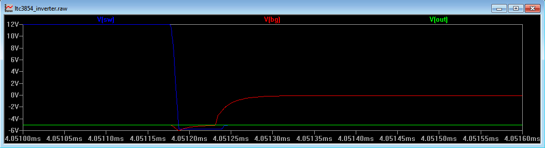
Figure 7
We can see the switch node (V(sw)) falling to a voltage below V(out) – in green - well before the drive to the bottom MOSFET gate starts to rise (in red). This is indicative of the body diode starting to conduct and indeed the negative voltage is approximately -0.6V. When the body diode conducts, it stores charge in the MOSFET that has to be removed before the MOSFET can fully turn on, so body diode conduction can affect the efficiency of the converter.
If optimum efficiency is desired, it is wise to place a Schottky diode across the bottom MOSFET, so the Schottky diode can conduct the inductor flyback voltage and not the body diode. The resulting increase in efficiency can be as much as 3%. The Schottky diode will conduct the peak current flowing through the inductor, but this current will only flow for a short period of time (until the bottom MOSFET switches on). Therefore, the current rating of the diode can be a lot less than peak inductor current. An MBRS340 has a reverse voltage rating of 40V, but a non repetitive peak forward current of 40A.
If optimum efficiency is desired, it is wise to place a Schottky diode across the bottom MOSFET, so the Schottky diode can conduct the inductor flyback voltage and not the body diode. The resulting increase in efficiency can be as much as 3%. The Schottky diode will conduct the peak current flowing through the inductor, but this current will only flow for a short period of time (until the bottom MOSFET switches on). Therefore, the current rating of the diode can be a lot less than peak inductor current. An MBRS340 has a reverse voltage rating of 40V, but a non repetitive peak forward current of 40A.
For the bottom MOSFET, the Renesas RJK0301 has 2.3mOhms RDSON and a Qg of 32nC.
Output Capacitor Choice
During the charging cycle of the inductor, the output capacitor has no current flowing into it, similar to a boost converter. Therefore the load current comes purely from the output capacitor. When the inductor discharges, the output capacitor it is subjected to an inrush current. If the capacitor has any ESR (effective series resistance) this will develop a ripple voltage on the output capacitor.
Therefore the output ripple is made up of 2 components: the ripple caused by the output capacitor discharging when the inductor is being charged and the ripple caused by the inrush current from the inductor into the ESR of the output capacitor.
The ripple caused by the discharge of the output capacitor while the inductor is charging is dictated by
where i is the load current in Amps, C is the output capacitance in Farads and dv/dt is the change in output voltage with time.
Earlier we calculated that the MOSFET switches on for a period of 725ns. If we require a discharge ripple of 0.5% (25mV) with a load current of 1A, this implies we need a capacitance of
or 29uF.
Note that when the inductor is charging, there is zero current flowing in the output capacitor. When the top MOSFET switches off, the bottom MOSFET current (and hence the capacitor charge current) jumps from 0A to the peak inductor current, so it is the peak inductor current, not the ripple current amplitude that determines this component of the output ripple (compare this with the ripple in a buck converter that is determined by the ripple current amplitude, not the peak inductor current).
The ripple caused by the ESR is a product of the peak inductor current and the ESR. In our example the peak current is 1.69A and the ESR is of a typical tantalum capacitor is 70m Ohms, giving a ripple of 118mV.
At this point is it worth trading off ESR ripple for discharge ripple and repeating the above two calculations on several combinations of output capacitor to see the effect on the ripple. We see that it is relatively easy to meet the spec of discharge ripple since our output capacitor is only 29uF. However if we are to achieve an overall output ripple of 1% (50mV) we are going to need lots of capacitors in parallel to meet the ESR required to keep the ESR ripple low.
Repeating the above calculations several times, it would appear that three 22uF capacitors in parallel will meet our overall ripple spec. 66uF will give a discharge ripple of 11mV and if each capacitor has an ESR of 70mOhms, the ESR ripple will be 39mV.
Other Points
The feedback resistor values can be calculated using this spreadsheet:
The final circuit is shown in Figure 8.
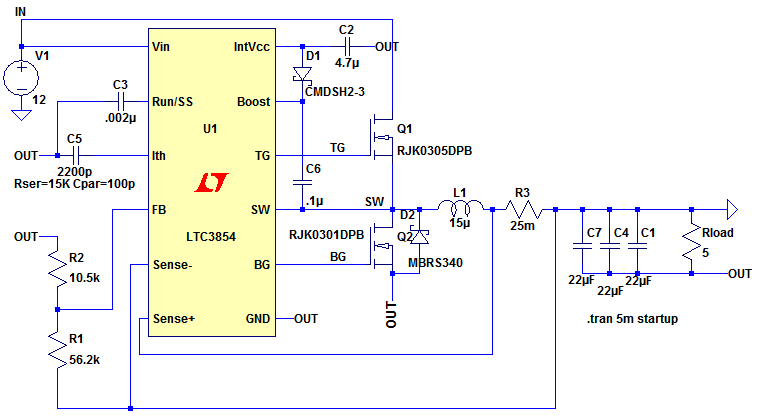
Figure 8
The LTspice circuit in Figure 8 can be downloaded here: Single Inductor Inverting dc/dc Converter
The Cuk Converter
In Figure 1 it can be seen that although the inductor current has a smooth charge/discharge, the input current (measured by holding down the ALT key and probing the input current into the controller) has sharp rise and fall times. This can lead to interference being generated in the circuitry supplying the input current. This is where the Cuk Converter provides a more suitable alternative.
The Cuk converter has an inductor on the input and the output, so both input and output currents have no sharp changes in current.
Figure 9 shows a Cuk Converter.
Figure 9
The LTspice Cuk Converter circuit above can be downloaded here: Cuk Converter.
It can be seen that the circuit about has the input configuration of a boost converter and the output configuration of a buck converter. However, unlike a boost or buck converter, the controller in a Cuk converter needs to be able to respond to a negative feedback voltage.
When MOSFET Q1 switches on, the right hand side of inductor L1 is shorted to ground. The current in the inductor ramps according to the equation
where V is the voltage across the inductor (in this case it is equal to the input voltage), L is the inductor value and di/dt is the change in inductor current with time. Thus with a fixed voltage across the inductor and a fixed inductor value, the change in current with time is constant. Thus in Figure 9 the change in current with time can be represented by
or 700,000 Amps per second.
When the MOSFET switches off, the inductor tries to maintain its current flow. It does this by creating a voltage across it where the right hand side tries to fly positive (to push current out of the right hand end) and the left hand side flies negative. Since the left hand side of the inductor is clamped to the input voltage, the right hand side of the inductor flies positive to a voltage above Vin in order to maintain current flow. The energy from the inductor flows into capacitor C5 charging it with a positive voltage (which is higher than Vin). The right hand side of C5 is clamped to +0.3V by diode D1, but for the sake of convenience we will ignore this voltage drop and assume the right hand side of the capacitor is clamped to 0V. We will work out later exactly what voltage C5 charges to, but for the moment it is sufficient to assume it charges to a voltage higher than Vin. We will call this voltage Vcap.
Since the voltage Vcap is higher than Vin, the voltage across the inductor now has the opposite polarity to before. The inductor discharges according to the equation
where V is the voltage across the inductor, thus
When the MOSFET switches on again the voltage on the drain of the MOSFET goes from Vcap to 0V. Since the voltage across a capacitor cannot change instantaneously, an equal negative going voltage appears on the anode of diode D1 so this node transitions from 0V to –Vcap. We now have a negative amplitude square wave voltage (at the right hand node of C5) being applied to an LC filter (L2 and C1). The LC filter averages out this square wave to produce a flat DC voltage whose amplitude is somewhere between 0V and –Vcap. This amplitude is dictated by the duty cycle of the square wave.
We are now going to calculate the duty cycle (the ratio of the ON time of the MOSFET to the total switching period) and the voltage (Vcap) on the coupling capacitor C5.
The inductor charge and discharge currents are equal when the circuit is in steady state. Therefore
where dt1 is the ON time of the MOSFET and dt2 is the OFF time of the MOSFET. Dividing both sides by (dt1+dt2) gives
If the Duty Cycle (DC) can be represented by
then
so
To determine the duty cycle in terms of the input and output voltages, consider Figure 10
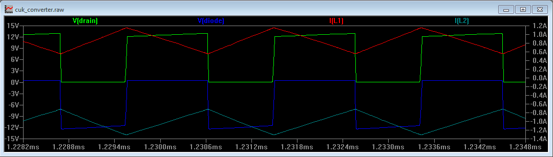
Figure 10
Here we can see the Drain voltage going from 0V to Vcap (as yet uncalculated) and the ac coupled drain voltage on the anode of the diode. The capacitor has removed the dc offset and the diode has clamped the positive excursions to roughly 0V.
Now, when the circuit is regulating there will be a flat negative dc voltage on the output. Thus, when V(diode) is at 0V there will be a positive voltage from V(diode) to V(out) and the inductor current in L2 will ramp in a positive direction. When V(diode) is negative there will be a negative voltage from V(diode) to V(out) so the inductor current will ramp to a more negative value.
In steady state, when the MOSFET switches ON V(diode) is at –Vc and the voltage across inductor L2 is (-Vout-(-Vcap)), thus the change in current is represented by
When the MOSFET switches OFF, the voltage across L2 is (0-(-Vout)), so the change in current is represented by
Equating the values of di gives
Dividing both sides by (dt1 + dt2) gives
where DC is the duty cycle as defined above.
Thus
From before we know that
So
So
Vout is the magnitude of the output voltage. This is because in the above derivation, we have ignored the slope of di – it is positive in L1 when negative in L2, so cannot strictly equate the 2 statements for DC without considering this.
The result of knowing Vcap is that we now know that the Drain of the MOSFET is exposed to a voltage equal to (Vin + |Vout|) and has to be sized accordingly (as does the capacitor’s working voltage).
Knowing that
and
We can work out the Duty Cycle in terms of Vout and Vin. Thus
Again, Vout is the magnitude of the output voltage.
The above is true as long as the current in the inductor does not fall to zero. This is called Continuous Conduction Mode (CCM). If the inductor current falls to zero, the duty cycle equation above does not hold and the controller enters Discontinuous Conduction Mode (DCM).
In CCM, if the load current increases, the duty cycle remains unchanged (in steady state). The circuit reacts to the increase in load current by keeping the duty cycle constant, but the midpoint of the inductor current (its dc offset) increases. The switching frequency and the amplitude of the inductor ripple current remain unchanged.
Cuk Converter Design Procedure
Our design brief is to design a Cuk Converter with an input voltage of 10V and an output voltage of 5V that can support a load of 1A. The switching frequency should be 300kHz.
Figure 11 shows a Cuk Converter based on the LT3757.
Figure 11
With a 10V input and a 5V output, we can calculate the duty cycle (DC) as being
With a switching frequency of 300kHz, this represents a period of 3.33us, so with a duty cycle of 33% the MOSFET ON time is 0.33 x 3.33us = 1.11us. The minimum ON time of the LT3757 is 220ns, so this is well within spec.
Inductor Choice
It is good design practice to keep the ripple current in the inductor at 40% of the total current. This is a good trade off between small inductor size and low switching losses. The inductor on the output of a Cuk Converter is configured identically to that of a buck converter. With the buck converter, the average inductor current is equal to the output current. On the input, the Cuk Converter has an inductor configured identically to that of a boost converter and the average inductor current in a boost converter is equal to the average input current.
With an output voltage of 5V and a load of 1A, this represents an output power of 5W. Allowing for an efficiency of 85% for the converter, this means our input power has to be 5.88W. With an input voltage of 10V, this represents an average input current of 588mA.
If the input inductor current ripple is 40%, then the peak inductor current is 588mA x 1.2, or 706mA and the trough inductor current is 588mA x 0.8, or 470mA.
The change in current is therefore 236mA.
From
when the MOSFET switches ON, the voltage across the input inductor is 10V, we have calculated that the ON time of the MOSFET is 1.11us, so we can work out the value of input inductance needed to get a change in current of 236mA. Thus
To calculate the output inductor value, we go through the same procedure.
We know that
and we know the voltage on the anode of D1 in Figure 11 is a square wave with amplitude of Vcap, we know that the output inductor has a voltage across it of Vcap – Vout (=Vin) when the MOSFET is ON, so for the same ON time our output inductor should be the same value as the input inductor for the same change in current. The purists would argue that since our output current is different to the input current then keeping both inductor values the same will result in a different ripple percentage in the output inductor, so the output inductor could be sized differently to reflect this, but the resulting change in circuit performance is minimal for most applications.
However, it should be noted that the current in the output inductor is considerably higher in this case (since we are stepping down the voltage, so stepping up the current). Therefore, if the average output inductor current is equal to the output current and we have a ripple current of 236mA, our peak output inductor current will be (1A + 118mA) = 1.12A.
So our input inductor needs to have a saturation current rating of at least 706mA and our output inductor needs to have a saturation current rating of at least 1.12A. It is convenient to select 2 identical inductors (for ease of purchasing), so two 47uH inductors with a saturation current of at least 1.12A are suitable.
If too much current flows in the inductor, the ferrite that the inductor is wound on saturates and the inductor loses its inductive properties. From the equation
if the inductor value falls, the current ramp increases causing the ferrite to further saturate… Therefore must make sure that the inductor never saturates.
The Wurth 744071470 is a 47uH inductor with a 1.3A saturation current.
Rsense Calculation
The current sense resistor calculation for a Cuk converter is different than that of the other dc/dc converter topologies. When the MOSFET switches on, the current flowing in the current sense resistor is equal to the sum of the two inductor currents (see Output Diode Choice for a further explanation). The sense resistor has to be scaled accordingly.
Thus with a peak sense current of 706mA + 1.12A (=1.83A) and a current sense trip threshold of 120mV (see LT3757 datasheet), a current sense resistor of 50mOhms should ensure good circuit operation.
On startup, when the MOSFET first turns on, there is a possibility that the peak current in the input inductor could ramp to well beyond its saturation rating. Given that we have a current sense resistor of 50mOhms and a sense voltage level of 120mV, it is conceivable that the peak current could reach 2.4A. However the LT3757 is fitted with a Soft Start function that gradually increases the peak current threshold comparator limit, determined by a capacitor on the SS pin. Appropriate sizing of this capacitor ensures the circuit’s output voltage has settled (thus the inductor currents have settled), before the threshold comparator reaches its full value.
MOSFET Choice
The MOSFET needs to be able to handle the peak current in both inductors (1.83A) so in this design a drain source current rating (Id) of 5A is more than sufficient. The Drain–Source voltage (Vds) needs to be in excess of Vcap (= Vin + |Vout|), so anything above 25V is suitable for a 10V input and -5V output.
The Gate-Source turn on voltage of the MOSFET (Vgs) needs to be less than the input voltage, to ensure that the voltage coming out of the Gate pin can actually activate the MOSFET. Logic level MOSFETs have a low turn on voltage, are widely available and usually perfect for low voltage dc/dc converters.
The above parameters represent the bare minimum characteristics of the MOSFET. However, to get a good design, we must ensure that the losses in the MOSFET are as low as possible. The MOSFET switch presents 2 losses in the circuit: Switching losses and conduction losses.
The switching losses result from current flowing through the MOSFET at the same time that a voltage is across the MOSFET (so power is generated in the MOSFET), during the turn on and turn off times of the MOSFET. For a given gate drive coming out of the controller IC, the lower the Gate-Source capacitance of the MOSFET, the quicker the MOSFET will turn on. Thus the Qg specification of the MOSFET is important and should be as low as possible. The Qg of the MOSFET will also have an impact on the heat dissipation of the chip, especially if the input voltage to the chip is high.
Charge is dictated by the equation:
Charge (Q) = Current (I) x Time (s)
Since Frequency is the inverse of Time, we can write
So we can calculate the current needed to flow into the IC, just to charge the gate capacitance of the FET. Since heat is the product of voltage and current, if the gate charge is high and/or the switching frequency is high, the heat dissipation in the chip will be high.
Once the MOSFET has switched on, the MOSFET presents a small dc resistance between its Drain and Source terminals. This is the MOSFETs ‘Drain Source on resistance’ or Rdson. Again, this needs to be as low as possible.
Now, MOSFET manufacturers reduce the ON resistance of the MOSFET by constructing many parallel conduction paths between the Drain and Source. Thus, like connecting resistors in parallel, the ON resistance comes down with more parallel paths. However, in connecting Drain Source paths in parallel, a negative effect is that the Gate Source capacitance (Qg) is also connected in parallel, so a low ON resistance (and hence low conduction loss) sometimes implies a high gate source capacitance (hence high switching loss). Thus the MOSFET that is chosen should be a compromise between these two characteristics. In addition, high current MOSFETs tend to come in much larger packages, so meeting the ideals of low ON resistance and low Qg might violate a space requirement spec, so the selection process has to start over. Engineering, as ever, is a compromise.
Indeed looking at the selection tables of the MOSFET manufacturers, it is better to select a MOSFET with a low ON resistance (less than 10mOhms), then filter this selection to remove MOSFETs with a Qg of greater than 10nC then select a MOSFET from this list, as long as the Gate turn on voltage, Vds and Id can be met. Starting by selecting MOSFETs with a Vds of between 20V and 30V might rule out some excellent devices and compromise the efficiency.
The Fairchild FDS6680 represents a good compromise between low ON resistance and low gate charge, but its SO8 package is large and therefore might be unsuitable for compact designs.
Output Diode Choice
The output diode needs to have the lowest voltage drop possible to give the lowest power dissipation (and hence the lowest loss). A Schottky diode is an ideal choice. During the input inductor charge phase, the diode is exposed to a reverse voltage of Vcap, which we have determined is equal to Vin + |Vout|, thus the reverse breakdown voltage of the diode should be higher than Vcap.
To calculate the diode current we need to first consider the current in the output inductor. The voltage on the anode of the diode oscillates from 0V (assuming 0V drop across the diode) to –Vcap where –Vcap is more negative than Vout. To keep a negative voltage on the output capacitor, the average current flowing in the output inductor must flow towards the diode (from right to left through L2 in FIG 11). If the ripple current in the output inductor is low compared to the average current, the current in L2 will not fall to zero so there will always be a current flowing in inductor L2 from Vout towards the diode.
When the MOSFET switches off, the current from the input inductor, L1, flows into the diode. In addition, the current from the output inductor will also flow through the diode. Therefore the total diode current during the discharge phase of the input inductor is equal to the peak current from both inductors. The diode current rating should be select accordingly. Our peak current is 1.83A, so the MBRS340 is a good choice.
Output Capacitor Choice
In continuous conduction mode, the capacitor has a continual current flowing into it from the output inductor. Unlike a boost converter, the output capacitor in a buck regulator does not have to hold up the output while the inductor is being charged.
The output is made up of 2 components: the ripple current from the output inductor producing a voltage across the effective series resistance (ESR) of the output capacitor and the ripple current charging the output capacitor according to the equation
Unlike a boost converter where the rectifier diode current jumps from 0A to the peak inductor current as the MOSFET switches off, the ripple in a buck architecture is determined by the ripple current amplitude, not the peak inductor current.
Recent innovations in ceramic capacitor design mean that very low ESR capacitors are available with high capacitance values. Ceramic capacitors have a typical ESR of 10mOhms.
Failing that, low ESR tantalum capacitors are available in much higher capacitance values with ESR of upwards of 50m Ohms. Of course capacitors can also be paralleled to increase the capacitance and reduce the ESR.
In our example the inductor ripple current is 236mA and the ESR is of a typical tantalum capacitor is 70m Ohms, giving an ESR ripple of 16.5mV.
To calculate the charging ripple, from the equation above we can see
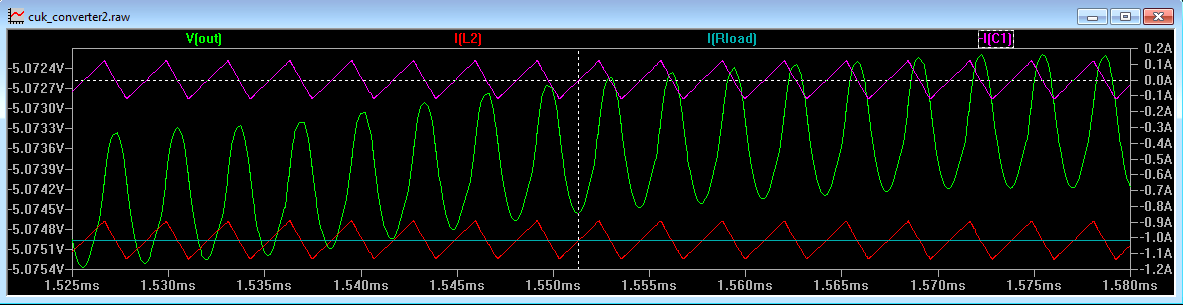
Figure 12
Figure 12, shows the output inductor ripple current (in red), output voltage ripple (in green) and output capacitor current (in purple). For convenience the output capacitor ESR has been reduced to 0 Ohms to fully illustrate the effect of discharge ripple. It can be seen that the capacitor current has the same amplitude as the inductor ripple current, but does not have the dc offset current (of approx. 1A). This is easy to picture, since the output current is equal to the average inductor current (i.e. a straight line drawn through the middle of the inductor current) and any current that does not flow into the load must flow in and out of the capacitor. To obtain the capacitor current, just subtract the output current.
Now, we can see that while the capacitor current is positive (above the dotted white line) the output capacitor voltage goes up and while it is negative, the output capacitor voltage goes down. To work out the amplitude of the ripple voltage on the output capacitor, we must calculate the average of the positive part of the capacitor current (above the dotted white line). Since we know the peak to peak ripple current (is equal to the inductor ripple current), the peak ripple current is Iripple/2 and hence the average of this current (since the current is triangular) is Iripple/4. We can now work out the charging ripple.
From
We can see that dt is equal to half the period, so we can say
Since our capacitor current is positive for half the ON time and half the OFF time, the above equation holds true regardless of duty cycle.
Let’s assume we want a ripple voltage of 1% (50mV). We already have 16.5mV of ripple as a result of the capacitor ESR, so we now have to have a charging ripple of 33.5mV
If our ripple current is 236mA and we are operating at a switching frequency of 300kHz, a capacitor of 3.3uF should suffice. Comparing this to the circuit in FIG 8, we can immediately see that for the same output current, the Cuk Converter has much less output capacitance. This is due to the fact that the output inductor current continually flows into the load whereas the output capacitor in the single inductor inverter has to keep the load current alive while the inductor is being charged.
Other Points
The feedback resistor values can be calculated using this spreadsheet:
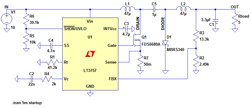
Figure 13
LTspice is a registered trademark of Analog Devices Inc
Sitemap: www.simonbramble.co.uk/sitemap
© Copyright Simon Bramble