Active Filter Design
Introduction
It’s a jungle out there. Somewhere in the dense wilderness, hidden from the view of the masses is a small tribe, much sought after by the head hunters of the surrounding plains. The tribe knows it is under threat and its numbers are dwindling at an alarming rate, killed off by the ever accelerating advancement of modern technology. This is the tribe of the Analogue Engineer.
Now every tribe has its elder, the one shrouded in mystique, who imparts wisdom while reminiscing of better days. Even in the tribe of the Analogue Engineer there is the guru - the rarest of the rare, the one you never get to see, even with an appointment. On the throne of his kingdom sits the Analogue Filter Designer. You call him ‘Sir’.
Many books have been written on active filter design and they normally include countless pages of equations that frighten most small dogs and some children. This article sets out to unravel the mystery of filter design and to allow the reader to design continuous time, analogue filters based on op amps in the minimum of time and with the minimum of mathematics.
The Theory of Analogue Electronics
There are two distinct sides to analogue electronics: the theory that the academic institutions teach (equations of stability, phase shift calculations) and the practical that most engineers use (tweak the gain with a capacitor to avoid oscillation). Unfortunately, active filter design is based firmly on long established equations and tables of theoretical values. Since designing practical circuits from theoretical equations can prove arduous, this text has derived the response of a general purpose filter 'building block' and translating the theoretical tables into practical component values involves nothing more than minor maths.
The Fundamentals
A simple RC Low Pass Filter has the transfer function
Cascading filters similar to the one above will give rise to quadratic equations in the denominator of the transfer function and hence further complicate the response of the filter. In fact, any second order Low Pass filter has a transfer function with a denominator equal to
and substituting different values of a, b and c determine the response of the filter over frequency. Now, anyone who remembers high school maths will notice that the above statement can have a value of zero for certain values of s, given by the equation
hence our transfer function can present infinite gain.
It is the points at which the quadratic equation in the denominator equals zero that the transfer function has theoretically infinite gain. These points are known as the poles of the quadratic equation and it is the values of these poles that establish the performance of each type of filter over frequency. These poles normally come in pairs and take the form of a complex number (a+jb) and its complex conjugate (a-jb) , although sometimes jb is zero.
In practice it is the real part, a, of the pole that indicates how the filter will respond to transients and the imaginary part, jb, that indicates how the filter will respond over frequency. We only ever apply frequencies to a filter, hence need not worry about the system going unstable.
This text will describe how to transfer the tables of poles found in many text books into component values suitable for circuit design.
Types of Filter
The three most common filter characteristics, and the ones discussed in this text, are Butterworth, Chebyshev and Bessel, each giving a different response. There are many others, but 90% of all applications can be solved with one of the above implementations.
The Butterworth implementation ensures flat response ('maximally flat') in the pass band and an adequate roll-off. This type of filter is a good ‘all rounder’, simple to understand and is good for applications such as audio processing.
The Chebyshev implementation gives a much steeper roll-off, but has ripple in the pass band, so is no use in audio systems. It is however, far superior in applications where there is only one frequency present in the pass band but several other frequencies that need removing (e.g. deriving a sinewave from a square wave by filtering out the harmonics).
The Bessel filter gives a constant propagation delay across the input frequency spectrum. Therefore applying a square wave (consisting of a fundamental and many harmonics) to the input of a Bessel filter will yield a ‘square’ wave on the output with no overshoot (i.e. all the frequencies will be delayed by the same amount). Any other filter will delay different frequencies by different amounts and this will manifest itself as overshoot on the output waveform.
There is the one more popular implementation, the Elliptical Filter, that is a much more complicated beast so won't be discussed in this text. Similar to the Chebyshev response, it has ripple in the pass band and severe roll-off at the expense of ripple in the stop band.
The Standard Filter Blocks
Figure 1a shows the generic filter structure and by substituting capacitors or resistor in place of components G1-G4, either a High Pass or Low Pass implementation can be realised. Considering the effects of these components on the op amp feedback network, it is quite easy to picture that a Low Pass filter can be derived from Fig 1a by making components G2/G4 into capacitors and G1/G3 resistors and vice versa for a High Pass implementation.
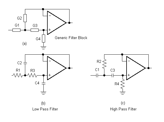
Figure 1
The transfer function of the Low Pass Filter shown in Figure 1b is
(to understand how this transfer characteristic was determined, please see the article on Nodal Analysis of Op Amps on this website).
Here the equation is simpler if conductances are used, where the capacitors have a conductance of sC and the resistors have a conductance of G.
If this looks too complicated, life is made much easier if the above equation is 'normalised'. This involves selecting either the resistors or the capacitors to be equal to 1Ω or 1F respectively and changing the surrounding components to fit the response. Thus, making all resistor values equal to 1Ω , the Low Pass transfer function is
This is the transfer function describing the response of our generic second order Low Pass Filter. We are now faced with taking the theoretical tables of poles describing the three main filter responses and translating these into real component values.
The Design Process
The designer should determine the type of filter required by selecting the pass band performance needed from the descriptions above. The simplest way of determining the desired order of the filter is to design a second order filter, then cascade multiple stages of this filter. Check to see if the implementation gives the desired stop band rejection, then proceed to design with the correct pole locations, shown in the tables in the appendix. Once the pole locations are established, the component values can soon be calculated.
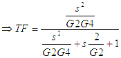
Firstly, each pole location needs to be transformed into a quadratic expression similar to that in the denominator of our generic second order filter. If a quadratic equation has poles of
When these are multiplied together, the resulting quadratic equation is
In the pole tables, a is always negative, so it is sometimes more convenient to use
and use the magnitude of a regardless of its sign.
To put this into practice, consider a fourth order Butterworth filter. Below are the poles of a fourth order Butterworth filter with the associated quadratic expression of each pole location. The poles can be found from the file at the end of this document.
From this, a fourth order Butterworth Low Pass Filter can be designed. Simply substitute the values from the above two quadratic expressions into the denominator of Equation 1.
Thus, in the first filter
C2C4 = 1; 2C4 = 1.8478 implying C4 = 0.9239F; C2 = 1.08F
and for the second filter
C2C4 = 1; 2C4 = 0.7654 implying C4 = 0.3827F; C2 = 2.61F
And all the resistors in both filters equal 1Ω.
Cascading both second order filters will yield a fourth order Butterworth response with a roll off frequency of 1 rad/s.
More realistic component values can be used while maintaining the same frequency response, as long as the ratio of the reactances to the resistors is maintained. Therefore one may elect to have 1kΩ resistors. Then divide the capacitor values by 1000 to ensure that the reactances increase in the same proportion as the resistances.
Unfortunately, we still have the perfect Butterworth response, but with a roll off frequency of 1rad/s. To change the frequency response of the circuit, we must ensure the ratio of the reactances to the resistors is maintained, but simply at a different frequency. Keeping the resistors at 1kΩ , for a roll off at 1kHz (rather than 1rad/s), the capacitor value has to be further reduced by a factor of 2π x 1000. Therefore the capacitors reactance does not reach our original (normalised) value until a higher frequency.
In conclusion, a fourth order Butterworth Low Pass Filter with a 1kHz roll off takes the form of Figure 2a
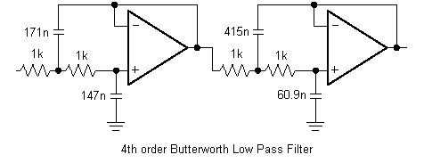
Figure 2a
Figure 2b shows the LTspice® plot of the output. Perfectly flat response in the passband and slow roll off after the break frequency.
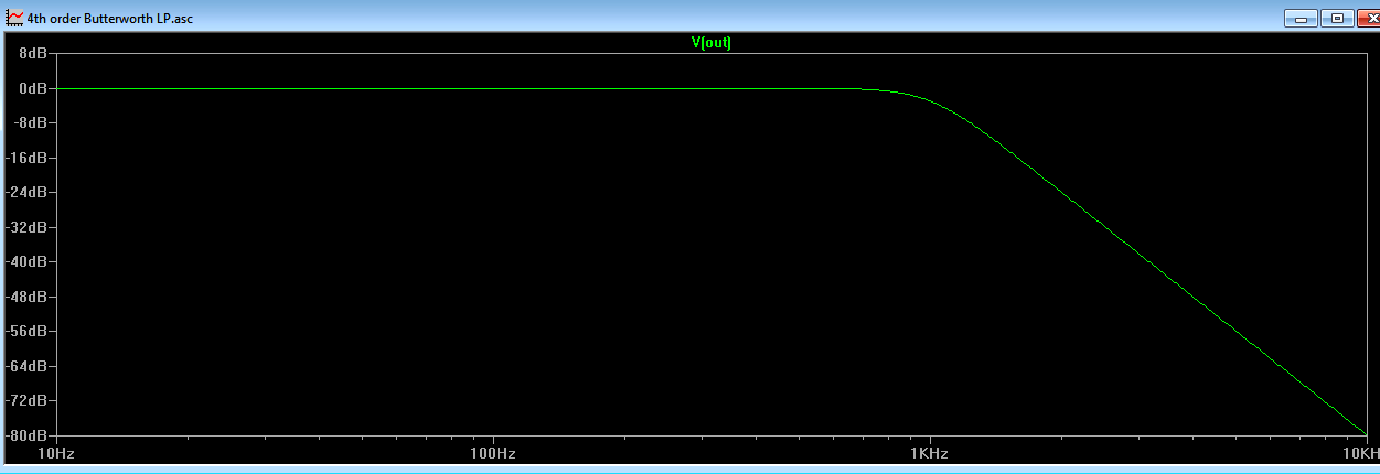
Figure 2b
Cascading any number of second order filters will obtain any even-order filter response using the above technique. At this point it is important to note that a true fourth order Butterworth filter is not simply obtained by calculating the components for a second order filter, then cascading two of these stages. Two second order filters have to be designed, each with different pole locations.
If the filter we are trying to design has an odd order, we can simply cascade second order filters, then add an RC network in the circuit to gain the extra pole.
For example, a 5th order, 1dB ripple Chebyshev filter has the following poles
The first two quadratics have been multiplied by a constant to ensure the last term equals unity, thus conforming to the generic filter described by Equation 1.
Thus, in the first filter
C2C4 = 2.488; 2C4 = 1.127 implying C4 = 0.5635F; C2 = 4.41F
and for the second filter
C2C4 = 1.08; 2C4 = 0.187 implying C4 = 0.0935F; C2 = 11.55F
Earlier in the text, it was shown that an RC circuit has a pole when
i.e.
Therefore to obtain the final pole at s = -0.28, a capacitor of C = 3.57F is needed if R = 1.
Normalising for a roll off frequency of 1kHz, using 1k resistors gives the circuit shown in Figure 3
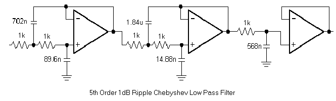
Figure 3
Thus the designer can now boldly go and design many Low Pass filters of any order at any frequency.
Now, all of the above theory can also be applied to the design of a High Pass Filter.
It has been shown that a simple RC Low Pass filter has the transfer function.
Similarly, a simple RC High Pass filter has the transfer function

Normalising these to correspond with the normalised pole tables gives:
and
 for a High Pass
It can be seen that the High Pass pole positions, s, can be obtained by inverting the Low Pass pole positions. Inserting the values into the High Pass Filter Block will ensure that the correct frequency response is obtained. To obtain the transfer function of the High Pass filter block, we need to go back to the transfer function of the Low Pass filter block. Thus from
interchanging capacitors and resistors it can easily be seen that the transfer function of the equivalent High Pass Filter Block is
Again, life is made much simpler if the capacitors are normalised instead of the resistors thus,
and putting
and
gives
This is the transfer function of the High Pass filter block and this time we calculate the resistor values instead of capacitor values.
Once the general High Pass filter response has been obtained, the High Pass pole positions can be derived by inverting the Low Pass pole positions and continuing as before.
Now, inverting a complex pole location is easier said than done. Take the example of the 5th order, 1dB ripple Chebyshev filter shown earlier. It has two pole positions at
(-0.2265 ±j0.5918)
The easiest way of inverting a complex number is to multiply then divide by the complex conjugate, to obtain a real number in the numerator. Finding the reciprocal is then a matter of inverting the fraction.
Thus
Gives
Inverting gives
The newly derived pole positions can then be converted into the corresponding quadratic and the values calculated as before.
We end up with
Thus from Equation 2 we can calculate the first filter component values to be
R2R4 = 0.401; 2R2 = 0.453 implying R2 = 0.227Ω ; R4 = 1.77Ω
This process can then be repeated for the other pole locations.
A simpler way to achieve the above is to design for a Low Pass filter using the suitable Low Pass poles, then treat every pole, s, in the filter as a single CR circuit since it has been shown that .
.
Inverting each Low Pass pole to obtain the corresponding High Pass pole simply involves inverting the value of CR. Once the High Pass pole locations have been obtained, we can interpose the capacitors and resistors to ensure the correct frequency response.
For clarification consider that so far, for the Low Pass implementation a normalised capacitor value was calculated assuming that R = 1Ω. Hence the value of CR is equal to the value of C. Finding the reciprocal of the value of C will find the High Pass pole and treating this as the new value of R will yield the appropriate High Pass component value.
Considering again the fate of the 5th order 1dB ripple Chebyshev Low Pass filter, the capacitor values calculated were:
C4 = 0.5635F; C2 = 4.41F.
To obtain the equivalent High Pass resistor values, invert the values of C (to get the High Pass pole location) and treat these as the new normalised resistor values. i.e. R4 = 1.77 and R2 = 0.227.
It can be seen that the same results are obtained as the more formal method mentioned earlier.
Thus the circuit in Figure 3 can now be converted into a High Pass Filter with a roll off at 1kHz by inverting the normalised capacitor values, interposing resistors and capacitors and scaling the values accordingly. Previously, the normalised Low Pass values were scaled by dividing by (2πfR). In this case, the scaling factor used is (2πfC), where C is the capacitor value and f is the frequency in Hertz.
The resulting circuit is thus
R2R4 = 0.401; 2R2 = 0.453 implying R2 = 0.227Ω ; R4 = 1.77Ω
This process can then be repeated for the other pole locations.
A simpler way to achieve the above is to design for a Low Pass filter using the suitable Low Pass poles, then treat every pole, s, in the filter as a single CR circuit since it has been shown that
Inverting each Low Pass pole to obtain the corresponding High Pass pole simply involves inverting the value of CR. Once the High Pass pole locations have been obtained, we can interpose the capacitors and resistors to ensure the correct frequency response.
For clarification consider that so far, for the Low Pass implementation a normalised capacitor value was calculated assuming that R = 1Ω. Hence the value of CR is equal to the value of C. Finding the reciprocal of the value of C will find the High Pass pole and treating this as the new value of R will yield the appropriate High Pass component value.
Considering again the fate of the 5th order 1dB ripple Chebyshev Low Pass filter, the capacitor values calculated were:
C4 = 0.5635F; C2 = 4.41F.
To obtain the equivalent High Pass resistor values, invert the values of C (to get the High Pass pole location) and treat these as the new normalised resistor values. i.e. R4 = 1.77 and R2 = 0.227.
It can be seen that the same results are obtained as the more formal method mentioned earlier.
Thus the circuit in Figure 3 can now be converted into a High Pass Filter with a roll off at 1kHz by inverting the normalised capacitor values, interposing resistors and capacitors and scaling the values accordingly. Previously, the normalised Low Pass values were scaled by dividing by (2πfR). In this case, the scaling factor used is (2πfC), where C is the capacitor value and f is the frequency in Hertz.
The resulting circuit is thus
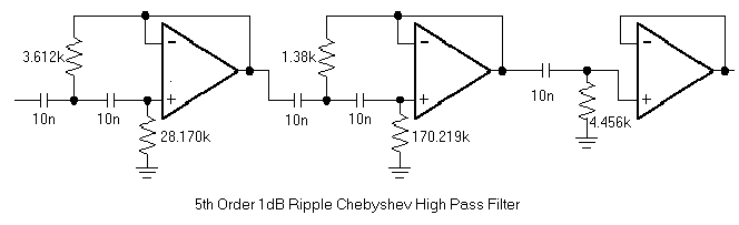
Figure 4a
Below we can see the LTspice schematic and transfer characteristic.
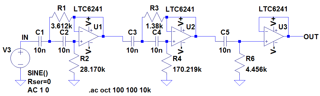
Figures 4b
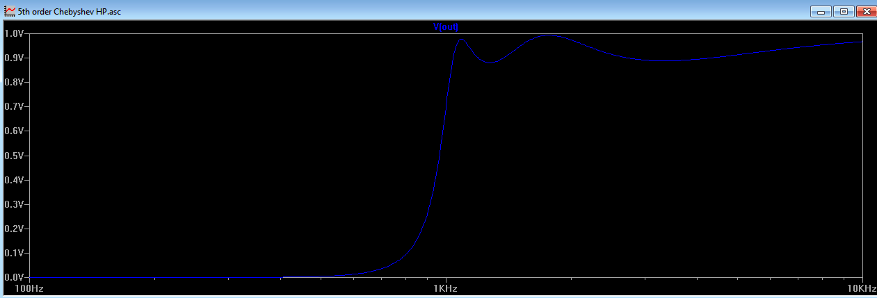
Figure 4c - The Frequency Response
Finally, just for kicks, let's implement a 9th order Chebyshev low pass filter with 1dB ripple, shown in Figure 5
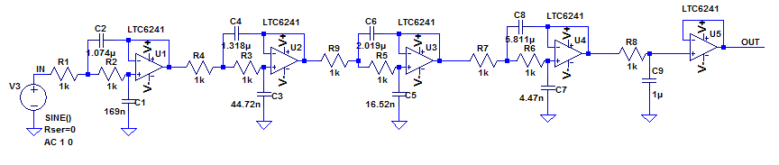
Figure 5a
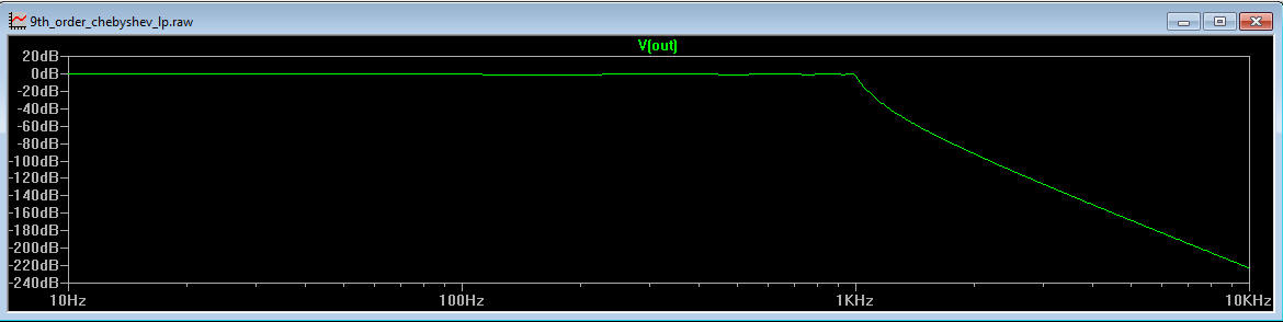
Figure 5b
and a close up on the ripple shows it is indeed 1dB
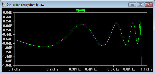
Figure 6
Please download the LTspice files and try them yourself:
4th Order Low Pass Butterworth
4th Order Low Pass Bessel
5th Order High Pass Chebyshev
9th Order Low Pass Chebyshev
Conclusions
Using the text above, the designer can now design Low Pass and High Pass filters with response at any frequency. Band Pass and Band Stop filters can be implemented with single op amps using techniques similar to those shown, but the scope of this article does not cover this. However, by cascading Low Pass and High Pass filters, both Band Pass and Band Stop filters can be implemented.
LTspice is a registered trademark of Analog Devices Inc
Sitemap: www.simonbramble.co.uk/sitemap
© Copyright Simon Bramble