Advanced Op Amp Tutorial
This article will explain advanced op amp behaviour including open loop gain, closed loop gain, loop gain, phase margin and gain margin. It expands on the (often incorrect) assumptions made about op amps that are only accurate at dc. The text includes simulations in LTspice®. If you are new to LTspice, tutorials can be found on this website.
Operational Amplifiers (Op Amps) are the cornerstone of analogue electronics. At low frequencies, the concepts of how an op amp works are very simple and their circuits are easy to analyse. However, the basics that are taught in most high schools only extend to the op amp’s performance at DC. At higher frequencies the basics are often not applicable and trying to analyse an AC circuit with DC design rules often leads to confusion.
This article will spend only the briefest of time looking at the DC characteristics of op amps then go on to explain how these characteristics change with increasing frequency.
The Ideal Op Amp
Text books teach that the ideal op amp has the following characteristics:
- Infinite input impedance
- Zero output impedance
- Zero dc input offset voltage
- Infinite gain
- Infinite bandwidth
While not every op amp has high bandwidth, infinite input impedance, zero output impedance and zero dc input offset voltage, it is fairly easy to find an op amp that will come close to these needs for a particular circuit application. However, no op amps have infinite gain or bandwidth and in fact the gain rolls off at very low frequencies and this has an effect on the assumptions made about the ideal op amp
The Op Amp at DC
A simple op amp circuit is shown in Figure 1. This has a non inverting gain of 10.
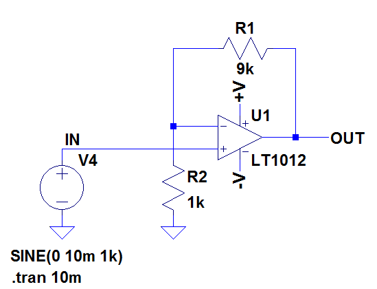
Figure 1
An LTspice version of this circuit can be downloaded here: Non Inverting Op Amp.
The gain of a non inverting op amp is given by
In Figure 1, RF is 9k and RI is 1k, so applying a 10mV peak input voltage to the non inverting terminal of FIG 1 implies a voltage of 10x that appears at the output, i.e. 100mV
Alternatively, if the 2 input terminals regulate to the same voltage, this creates a current of 10uA through R2. This current can only come from the output (as the input terminals do not source current) meaning that R1 needs to develop a voltage of 90mV, meaning the output voltage will be at 90mV + 10mV = 100mV.
Looking at this circuit another way, there is a potential divider from the output back to the inverting input. If the circuit regulates to keep the 2 inputs the same, then
so
So there are a number of ways of determining the gain of an op amp.
Now, it is always assumed that the two input terminals are at the same voltage (ignoring the dc offset voltage). In fact the voltage across the input terminals is made up of two components: the dc offset voltage and a much smaller component that is dependent on the open loop gain of the amplifier and it is this second component that most people ignore which leads to confusion when analysing the op amp at ac.
The Op Amp at AC Frequencies
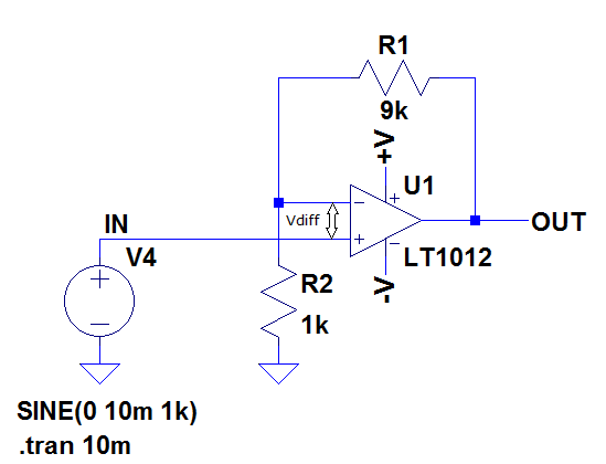
Figure 2
In the following paragraphs, for the sake of clarity, we will assume that the input offset voltage of the amplifier is zero. The open loop gain of the amplifier is equal to the output voltage divided by the differential voltage across the 2 inputs (in Figure 2 this is the voltage at the OUT node divided by the voltage Vdiff). The closed loop gain is equal to the voltage at the OUT node divided by the voltage at the IN node, as discussed above. Regardless of the circuit configuration, the op amp always operates in open loop gain. As circuit designers, we choose to put components around the amplifier to give us a certain closed loop gain, but the amplifier always tries to amplify the voltage Vdiff by its open loop gain to give a voltage at the OUT node.
Another way of looking at this is that for any given voltage at the OUT node, there will be a very small voltage, Vdiff, across the input nodes whose magnitude is equal to V(OUT) divided by the open loop gain. In op amp theory taught in school, the open loop gain is assumed to be infinite, so the differential voltage, Vdiff is then infinitely small (zero). As long as the open loop gain of the amplifier remains high, this voltage is much smaller than the input voltage and can be ignored. However, if the open loop gain of the amplifier goes down, this voltage starts to get bigger and this is discussed below.
The open loop gain is assumed to be infinite and although it is very high at dc, it rolls off soon after DC and this affects the AC performance of the op amp. The open loop characteristic of the LT1012 is shown in Figure 3a
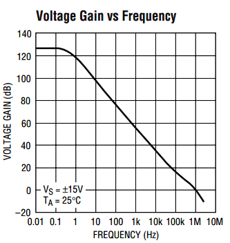
Figure 3a
The LTspice plot of this is shown in Figure 3b with the solid green line showing the gain and the dotted green line showing the phase. The LTspice circuit can be downloaded here: Open Loop Op Amp Characteristics
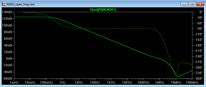
Figure 3b
At frequencies below about 0.3Hz the open loop gain is high at about 126dB (about 2 million). Beyond 0.3Hz, the open loop gain starts to roll of at 20dB per decade increase in frequency meaning that the open loop gain goes down by a factor of 10 for every tenfold increase in frequency. This roll off is exactly the same as a simple RC filter with a cut off frequency at 0.3Hz where the response decays at 20dB per decade above the cut off frequency.
If
If
then to maintain a certain output voltage at V(OUT), if the open loop gain starts to decrease, the input voltage Vdiff has to increase.
At low frequencies the voltage Vdiff in Figure 2 will be small due to the high open loop gain of the op amp. However, at higher frequencies (above 0.3Hz), the voltage Vdiff gets bigger and bigger as the open loop gain gets smaller and smaller.
In Figure 4a a 10mV signal is applied to the circuit in Figure 2 and a 100mV signal appears at the output, so we have a gain of 10 as expected. With an input frequency of 0.01Hz the differential voltage, Vdiff, measured across the input is 52nV. We can see from Figure 3a that the open loop gain of the amplifier at 0.01Hz is approximately 126dB (2 million) thus Vdiff should be 100mV divided by 2 million (50nV) which it is.
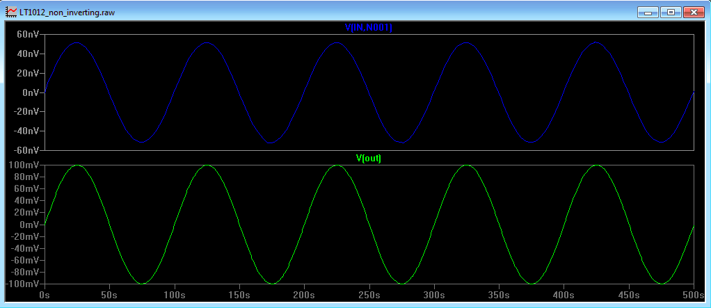
Figure 4a
In Figure 4b, the frequency is increased to 1Hz and all other circuit parameters remain unchanged. From Figure 3a, we can see that the open loop gain of the op amp is about 115dB (about 550,000). This is slightly easier to see in Figure 3b. The differential voltage, Vdiff, measured across the input is now 182nV. This corresponds to the output voltage (100mV) divided by the open loop gain at 1Hz (550,000). Notice also that in Figure 4a both waveforms are in phase whereas in Figure 4b there is a phase shift between the input and the output.
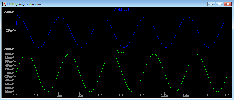
Figure 4b
In Figure 4c, the frequency is increased to 100Hz. The open loop gain of the op amp at 100Hz is 75dB (5700). The differential voltage measured across the input is 17.5uV which corresponds to the output voltage (100mV) divided by the open loop gain at 100Hz (5700). The output voltage is also phase shifted with respect to the input.
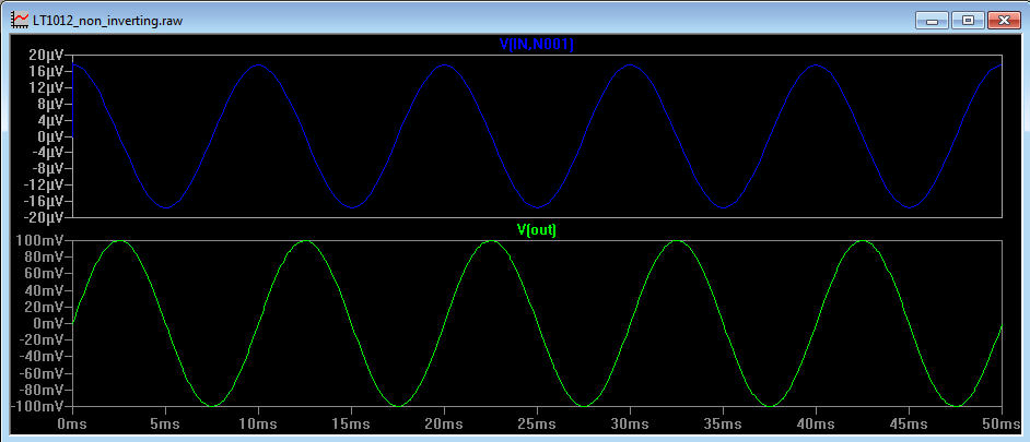
Figure 4c
Just for completion, changing the feedback resistor in Figure 2 from 9k to 99k gives the amplifier a gain of 100. Figure 4d shows the effect on the output and the differential voltage.
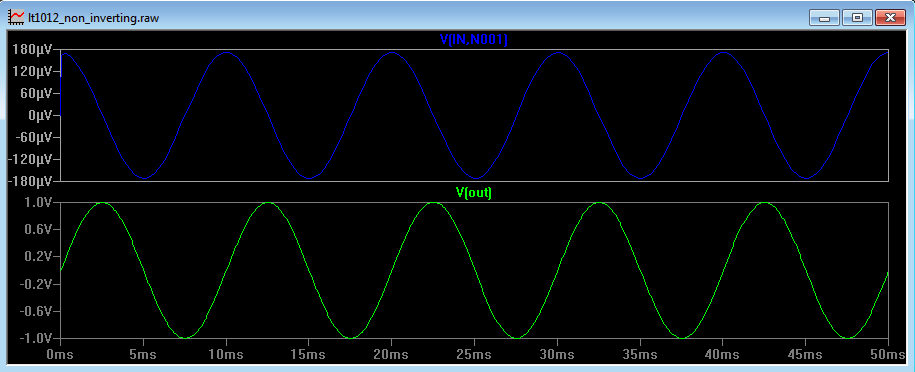
Figure 4d
The output has increased by a factor of 10 (as expected), but so has the differential voltage. This is to be expected since the op amp’s open loop gain remains unchanged at a given frequency. If the output voltage increases by a factor of 10, for a given open loop gain, this means the differential input voltage also has to increase by a factor of 10. This will have important implications and these will be explained later.
It is interesting to note that although the LT1012 has a very low offset voltage, the simulation model appears to have a virtually zero dc input offset voltage which makes our analysis much easier.
Thus it can be seen that the differential input voltage increases with decreasing open loop gain and the output undergoes a phase shift above 0.3Hz which is the frequency at which the open loop gain starts to roll off (the break frequency).
It should also be noted that, like a simple RC filter, the phase shift occurs at frequencies around the break frequency. For a single order RC filter (one where the gain falls at 20dB per decade) the phase shift will only ever get to 90 degrees. Figure 4c shows a phase shift of 90 degrees and if we were to increase the frequency above the 100Hz shown in Figure 4c, the phase shift would stay at 90 degrees.
We can see from Figure 3 that the slope of the open loop gain changes above 1MHz and starts to decay at more than 20dB per decade. This effect is similar to a second RC filter with a break frequency of 1MHz. This second RC filter will introduce a further 90 degrees phase shift resulting in a 180 degrees phase shift at frequencies well in excess of 1MHz.
It is important to remember that although Vdiff is phase shifted with respect to the output, its amplitude is only very small compared to the input voltage of 10mV. The voltage at both input terminals is still approximately 10mV and as long as Vdiff is small compared to the input voltage, we need not worry too much about the phase shift.
Phase Shift
The LT1012’s open loop gain has the frequency response of a single order low pass filter. A similar low pass filter (this time with a break frequency of 1kHz) is shown in Figure 5.
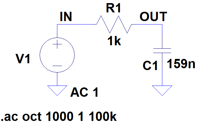
Figure 5a
An LTspice simulation of this circuit can be downloaded here: First Order Low Pass Filter.
This filter’s frequency response can be seen in Figure 5b. The break frequency occurs when the output is 3dB lower than the input as represented by the solid green line below and read off the left hand axis.
This filter’s frequency response can be seen in Figure 5b. The break frequency occurs when the output is 3dB lower than the input as represented by the solid green line below and read off the left hand axis.
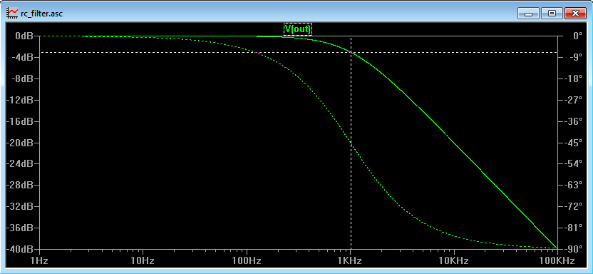
Figure 5b
For a single order low pass filter the phase shift at the break frequency is 45 degrees, as represented by the dotted green line above and read off the right hand axis. As an approximation, for a first order low pass filter, the phase shift at 10x less than the break frequency is about 0 degrees and at 10x greater than the break frequency, the phase shift is 90 degrees and this can be seen in Figure 5b.
A mathematical derivation of the amplitude and phase shift can be seen here: Low Pass Filter Amplitude and Phase Shift
A low pass filter has a phase lag response. This means the output voltage reaches its peak after the input voltage and this can be seen in Figure 4c above, although it is not immediately obvious. The voltage at the non inverting input is the forcing function so is at zero phase. The signal passes through the op amp and undergoes a phase lag and this appears at the inverting input. The blue waveform in Figure 4c is measured from the non inverting terminal to the inverting terminal and clearly leads the green waveform. Therefore if the blue waveform were measured from the inverting terminal to the non inverting terminal it would be lagging the green waveform.
Figure 6 shows a similar 2 pole filter with one pole at 1kHz and one at 100kHz. It can be seen from Figure 7 that the first pole introduces a roll of at 20 dB per decade and worst case 90 degree phase shift as expected and the second pole introduces a further 20 dB per decade roll off and another 90 degree phase shift.
At the first break frequency the phase shift will be 45 degrees and at the second, it will be 135 degrees (90 degrees + 45 degrees).
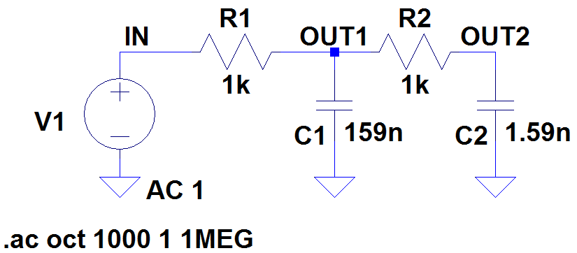
Figure 6
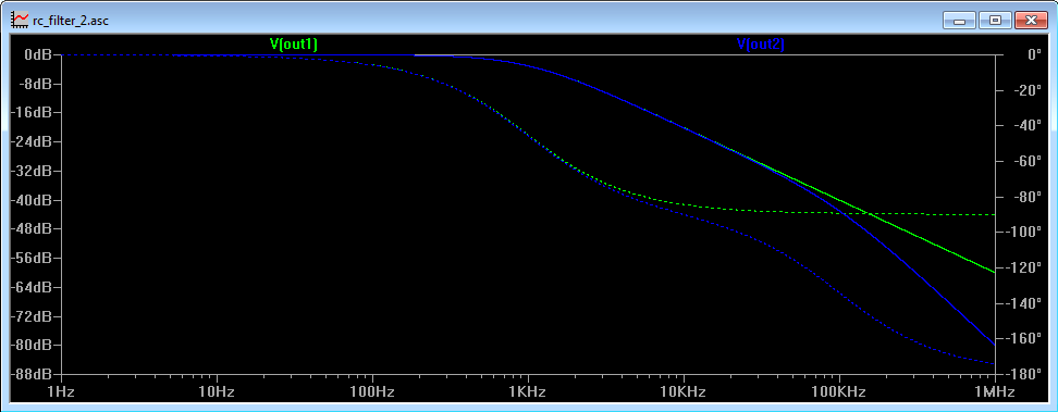
Figure 7
Some amplifiers, including the LT1012 exhibit an open loop characteristic with 2 break frequencies (similar to that in Figure 7). With the LT1012, the first break frequency is at 0.3Hz so introduces a 45 degree phase shift at 0.3Hz (and a 90 degrees phase shift at frequencies above 3Hz) and the second break frequency is at 1MHz, at which point the open loop characteristic will have a 135 degrees phase shift. The open loop phase shift will tend towards 180 degrees as the frequency gets towards 10MHz.
Loop Gain
A general feedback system, like most op amp circuits, is represented in Figure 8.
Loop Gain
A general feedback system, like most op amp circuits, is represented in Figure 8.
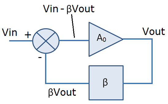
Figure 8
The ‘+’ and ‘-‘ inputs represent the non inverting and inverting inputs to the op amp. The gain block A0 represents the open loop gain of the amplifier and β is the fraction of the output fed back (via the feedback and input resistors). It can be seen that
so
so
so
If A0 is large then the overall closed loop gain approximates to
since βA0 is large compared with ‘1’ and the A0 on the numerator and denominator cancel. Therefore the gain of the system approximates to the reciprocal of the feedback fraction (β).
This can be seen in Figure 1. The feedback fraction is a simple resistive divider represented by
so the overall gain is 10.
We are now going to introduce the concept of Loop Gain. It should be noted that loop gain, open loop gain and closed loop gain are 3 different parameters and should not be confused. Loop gain is not something that is measured in everyday electronics, but it is useful in explaining how op amps might start misbehaving at high frequencies.
Referring to Figure 2 we know that open loop gain is defined as:
And closed loop gain is defined as
We are now going to define loop gain as the open loop gain, A0, multiplied by the feedback fraction, β i.e. the gain going around the loop. This is easy to picture in Figure 8.
If the loop gain is equal to βA0 and we know that the closed loop gain approximates to 1/β, we can say that the loop gain approximates to the Open Loop Gain divided by the Closed Loop Gain (i.e. βA0 is equal to A0 divided by 1/β) , which is equal to
In other words, the loop gain is a measure of how big the input voltage, V(IN), is compared with the differential voltage, Vdiff. However, this is only an approximation.
To find the exact value of the loop gain, we need to examine Figure 8. Looking at Figure 8, (Vin – βVout) is actually the same as Vdiff in Figure 2 (the differential voltage across the 2 op amp inputs). Since the loop gain is the feedback fraction (β) multiplied by the open loop gain (A0) we can see from Figure 8 and Figure 2 that the exact value of loop gain is the voltage at the inverting terminal, not V(IN), divided by the differential voltage, Vdiff.
We have seen from the plots of Figure 4 that the voltage difference between the inverting terminal and the non inverting terminal gets bigger as frequency increases implying that our approximation of the loop gain equalling V(IN)/Vdiff is only accurate when Vdiff is small.
We would not normally measure the magnitude of the input voltage and compare it with the differential voltage, so why is this of any use?
Well, we can see in Figures 4a - 4d that if the voltage Vdiff is small compared with V(IN) then it presents no problem and can be ignored. From the equation above, this represents a high loop gain. However, if Vdiff starts to become comparable to V(IN) (as loop gain reduces) it will start to interfere with the input signal and can no longer be ignored.
We have already seen in Figure 3 and Figure 5b that if the op amp has a first order response (i.e. the open loop gain rolls off at 20dB per decade and the phase shift is no higher than 90 degrees) that this is not a problem. However, if the op amp has a second order response as shown in Figure 7 then it is possible that the phase of Vdiff can be close to 180 degrees out of phase with the input at high frequencies. Again this is not normally a problem if Vdiff is small compared with V(IN), but if Vdiff is comparable in magnitude with V(IN), then we are nearing a point of potential oscillation.
Put another way, under normal circumstances the voltage fed back is applied to the inverting input so opposes the input signal. However, if this voltage is inverted through the amplifier (in Figure 8 this is the A0 block), the feedback signal appears in phase with the input signal and there is a potential for oscillation.
Plotting the closed loop gain on the graph shown in Figure 3, we get the graph of Figure 9 with the closed loop gain shown in red.
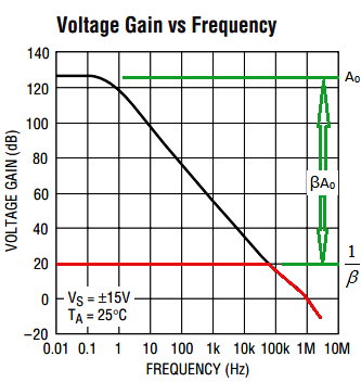
Figure 9a
We can also see this plotted in LTspice in Figure 9b
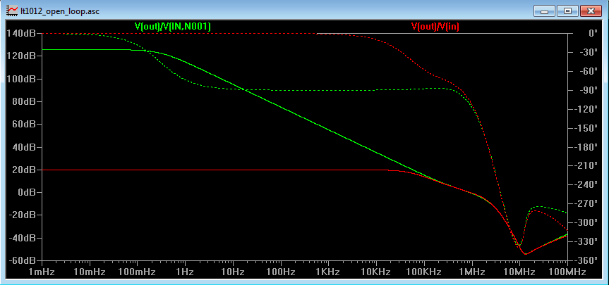
Figure 9b
The Open Loop Gain is at roughly 125dB and is represented by A0 and the Closed Loop Gain is 20dB and is represented by 1/β as seen by the red line in the logarithmic plots in Figure 9a and Figure 9b.
Now, the difference between two numbers on a logarithmic plot is equal to the ratio of the two numbers on a linear plot.
We have already established that the Loop Gain approximates to the Open Loop Gain divided by the Closed Loop Gain, so on a logarithmic scale, this is represented by the difference between the Open Loop Gain plot and the Closed Loop Gain plot (i.e. the distance between the open loop curve and the closed loop curve below it) as indicated in Figure 9a.
So the ratio of open loop gain to closed loop gain is

Thus the distance between the open loop curve and the closed loop curve is βA0 which represents the Loop Gain. βA0 is the loop gain of the system.
Phase Margin and Gain Margin Explained
In Figure 10, consider a signal, Va, applied to the input of the amplifier, A0. It passes through the amplifier then through the feedback network, β and arrives back at the differential input stage (Vb). At this point it is inverted by the differential stage. If Va is subjected to a 180 degrees phase shift when passing through the gain stage A0 and then inverted by the differential stage, it will now be back in phase with the original signal.
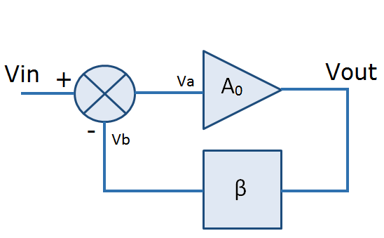
Figure 10
If at a given frequency the amplitude of Vb is greater than or equal to the amplitude of Va, then there is a possibility that the system will oscillate. Under these conditions, the system needs no external voltage at Vin to produce a sustained voltage at Va and Vb . Looking at Figure 10, we can see that Vb is equal to Va x βA0, where βA0 is the loop gain of the system, so we can now see why loop gain is important in determining the stability of a feedback system. If βA0 has a phase shift of 180 degrees and a magnitude of greater than 1 the circuit will oscillate.
This can be related back to the equation
This can be related back to the equation
If the loop gain, βA0 has a phase shift of 180 degrees (i.e. is negative) and has reduced to unity at a certain frequency, the denominator of the above equation reduces to zero and the circuit will oscillate at that frequency.
For the loop gain to equal unity, the Closed Loop Gain equals the Open Loop Gain, since the loop gain is defined by Open Loop Gain divided by Closed Loop Gain. It can be seen that the stability of a system can thus be determined by looking at the point where the Open Loop Gain and Closed Loop Gain meet. This is where the loop gain equals unity.
Figure 11a shows the open loop response of anther op amp, the LT1226. It can be seen that at an open loop gain of 20dB we have a phase shift of 180 degrees (where the dotted white line crosses the dotted green line and reading off the right hand axis). This occurs at 65MHz. So potentially there could be a problem using the LT1226 with gains of less than 20dB. Figure 11b shows the circuit – a non inverting gain of 100 with an input voltage of 10mV. This Open Loop test circuit can be downloaded here: LT1226 Open Loop Circuit
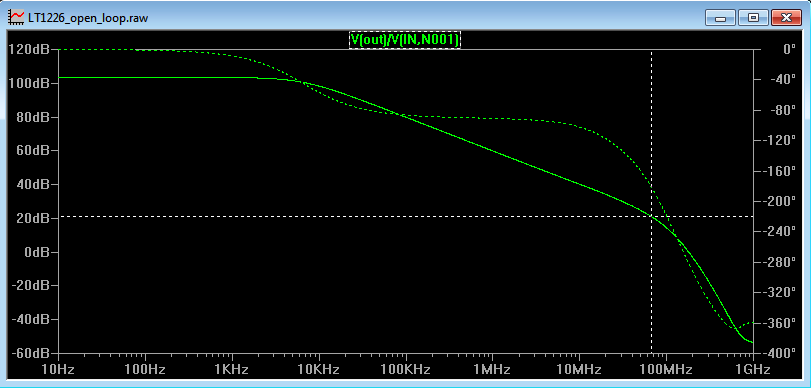
Figure 11a
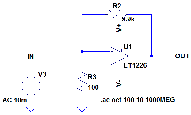
Figure 11b
Figure 11b
The open loop gain of the LT1226 has its first break point at 6.5kHz (where the roll off is at 20dB per decade) and a second one at about 30MHz where the slope changes from 20dB per decade to 40dB per decade. At frequencies of 10x less than 6.5kHz, the phase shift approximates to zero and at frequencies 10x higher than 6.5kHz, the phase shift approximates to 90 degrees. At 6.5MHz the phase shift is 45 degrees.
Figure 12 shows an input signal of 65kHz (10x higher than the open loop break frequency). Here we can see that the differential voltage between the op amp inputs is phase shifted by 90 degrees with respect to the output voltage. Remember that the open loop gain is V(OUT)/Vdiff, so the comparison we are making in Figure 12 should correspond to the phase shift of the open loop gain. Indeed Figure 11a shows the open loop gain of the LT1226 and we can see that at 65kHz the phase shift is indeed 90 degrees.
This circuit can be downloaded here: Non Inverting LT1226 Circuit
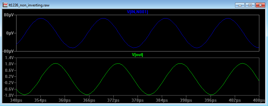
Figure 12
We can see that the voltage Vdiff (65uV) is small compared to the 10mV input signal, so the output signal is at the amplitude we expect (1V), for a circuit with a gain of 100.
Increasing the frequency by a factor of 1000 to 65MHz, the open loop gain is 21dB (about 11) and the phase shift is 180 degrees, from Figure 11a. Inputting a signal of 65MHz gives the results of Figure 13
Increasing the frequency by a factor of 1000 to 65MHz, the open loop gain is 21dB (about 11) and the phase shift is 180 degrees, from Figure 11a. Inputting a signal of 65MHz gives the results of Figure 13
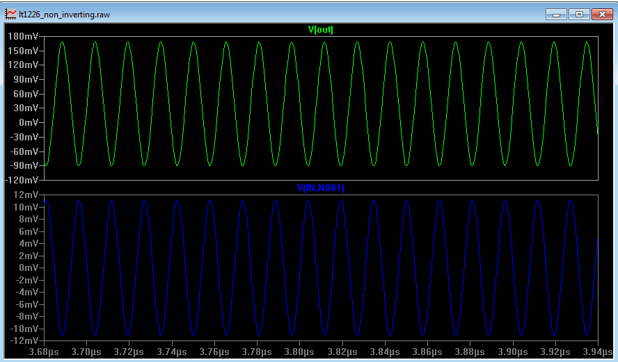
Figure 13
We now have a phase shift of 180 degrees of Vdiff with respect to the output. So why is the circuit not oscillating? For a circuit to oscillate, we need a phase shift of 180 degrees around the loop as well as gain. We have the phase shift, but do we have enough gain? We now need to look at the signal at each of the input terminals to see if there is enough gain in the loop. So far we have looked at the voltage across the 2 op amp inputs (Vdiff), because it is easier to measure a Vdiff of, say, 100nV rather than measure the input voltage of 10mV and the voltage at the inverting terminal which is (10mV – 100nV). To get a true idea of instability we have to measure the voltage at each input.
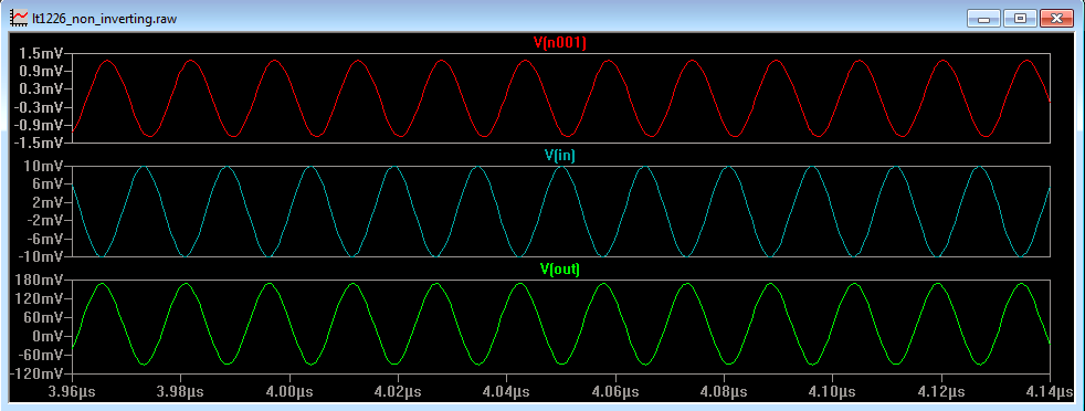
Figure 14
Figure 14 shows the voltage at the inverting terminal (V(n001)), the input and the output. The input is at 10mV, but the output voltage has suffered because of the poor open loop gain of the amplifier. Indeed measuring the voltage at the output pin and dividing it by the differential voltage across the inputs, we should still arrive at the open loop gain figure of approximately 21dB. It should be noted that there is a 40mV output offset voltage that should be removed from the output voltage reading before calculating the gain.
Looking at the voltage at the inverting terminal, we can see that it is one hundredth of the voltage at the output and it is in phase with the output voltage. This is to be expected as there is a resistive divider (that gives zero phase shift) from the output back to the inverting terminal made up of resistors R2 and R3 and giving an attenuation of 100 as seen in Figure 11b.
We can also see that the voltage at the inverting terminal (V(n001)) is substantially lower than the input voltage, so although it is out of phase with the input by 180 degrees, it is not bigger than V(IN) so the system cannot oscillate.
Now, we can reduce the gain of the amplifier by reducing, for example, the feedback resistor R2 in Figure 11b. In doing so the attenuation effect of the resistors R2 and R3 gets less, so more voltage appears at the inverting input. Thus it can now be seen that at a given frequency where the voltage at the inverting terminal is inverted with respect to the voltage at the non inverting terminal, decreasing the gain is not a good idea, as this will increase the voltage at the inverting terminal. Ultimately we will reach a point where the voltage at the inverting terminal is 180 degrees out of phase and greater in amplitude than the voltage at the non inverting terminal. We now have a condition for oscillation. This is why many op amps have a minimum gain stability. If the gain is reduced below this point, the op amp will start to oscillate. This can be seen in Figure 15.
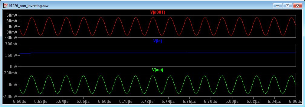
Figure 15
Here R2 has been reduced to 1k and R3 kept at 100 Ohms and this has caused an increase in the voltage at the inverting input. This voltage is higher in amplitude than the 10mV input signal, so we can remove the 10mV input signal and the circuit will continue to oscillate. This can be seen in Figure 15. (The input frequency has actually been reduced to 1Hz).
The output voltage has a peak to peak amplitude of 1.049V and the inverting input has an amplitude of 94.67mV. The feedback fraction is 100/(100+1000) = 0.091. If the non inverting terminal is at 0V, then the differential voltage is at 94.67mV. We can work out the open loop gain to be 1.049V/94.67mV = 11.08. Thus the feedback fraction multiplied by the open loop gain is 0.091 x 11.29 = 1.01. Thus we have 180 degrees phase shift with a loop gain of >1 and these are the conditions for possible oscillation.
Gain and phase margin are a measure of how close to the point of oscillation the circuit is. In other words how close to 180 degrees phase shift or unity gain the loop gain is. It is a measure of the loop gain of the circuit, not the closed loop gain or the open loop gain.
Phase margin is a measure of how close the loop gain is to having 180 degrees of phase shift when the loop gain is unity. If βA0 has 180 degrees of phase shift when it has a magnitude of unity, the circuit has zero degrees of phase margin and will oscillate. If the loop gain has a phase shift of 160 degrees, the circuit has a phase margin of 20 degrees.
Gain margin is a measure of how far below unity the loop gain of the circuit gain is when the loop gain, βA0, has a phase shift of 180 degrees. If the loop gain has a phase shift of 180 degrees and a loop gain of 0.6, the circuit has a gain margin of 0.4. A circuit with a loop gain of 0.8 has a gain margin of 0.2 and hence is nearer to the point of oscillation.
LTspice is a registered trademark of Analog Devices Inc
Sitemap: www.simonbramble.co.uk/sitemap
© Copyright Simon Bramble