Nodal Analysis of Op Amps
Introduction
There is little doubt that the op amp is the most fundamental of all analogue components and its creation marked a change in the whole thinking behind analogue electronics. Since it is such a widely used device, pretty much any op amp circuit that the engineer needs to implement has already been designed and he is faced with merely tailoring the component values to suit his needs. This approach, although quick, does not always mean the designer has a fundamental understanding of the theory of the circuit operation. This article will set out to explain, by the simple process of nodal analysis, how the transfer function of most op amp circuits can be derived.
The Basics
It is clear that no electronic component is perfect and the op amp is no exception. However, to keep things simple, an ideal op amp has been used, but as with other things in life the ‘supermodel’ is going to be admired but with constant awareness of the flaws that lie under the façade.
For the following text, the perfect op amp is one with infinite input impedance and zero output impedance. Thus the front end of the circuit is not loaded in any way by the op amp and its output can source or sink as much current in response to the input. In most op amp configurations with negative feedback, the voltage at the two inputs is identical and the output adjusts itself to a voltage to maintain this state. It is also assumed that the bandwidth of the op amp is sufficient to respond to the needs of the circuit and the open loop gain of the amplifier is infinite. Now, the designer could continue to assume many things about his design and end up with a circuit that he can only assume will never work. However, with real life components the above assumptions are perfectly acceptable and very little circuit degradation occurs in moving away from the ideal.
Nodal Analysis
It was a long time before the op amp was invented that Kirchoff devised Kirchoff’s law stating that the current flowing into any junction (or node) of an electrical circuit is equal to the current flowing out of it. Any op amp circuit can be broken down into a series of nodes, all of which will have a nodal equation related to them. These can then be combined to form the transfer function.
Considering the circuit at the input of an op amp, this means that the current flowing towards the input pin is equal to the current flowing away from the pin, since no current flows into the pin due to its infinite input impedance. However, it is worth noting that the same cannot be said for the output since the op amp will change the current it sources or sinks in order to keep the two inputs of the op amp the same.
Current to Voltage Converter
Putting this to the test, consider the fate of a simple current to voltage converter (Figure 1). The input current flows towards the node at the inverting pin. The current flowing into this node is equal to the current flowing away from the node, so current flows through the feedback resistor, R, since no current flows into the pin. Thus a voltage is developed across R (= Iin x R) and the output adjusts in sympathy to keep that current flowing. From our assumptions in the previous paragraph, the voltage at the two inputs must remain the same. If the non inverting input is at 0V, the output will start at 0V and decrease for an increasing current input current, to maintain current flow.
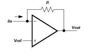
Figure 1
Differential Amplifier
Taking this notion one stage further, Figure 2 shows a differential amplifier. It transfer function can be calculated by again considering the currents flowing into and out of the nodes.
Taking this notion one stage further, Figure 2 shows a differential amplifier. It transfer function can be calculated by again considering the currents flowing into and out of the nodes.

Figure 2
Firstly consider the current flowing towards the non inverting pin. This can be represented by:
Similarly, current flowing away from that node can be represented by
Combining Equation 1 into Equation 2 gives
Now, the maths is made easier if we use conductances instead of resistances (it keeps the fractions to a minimum).
Thus
where
and
so
therefore the voltage V+ is given by
The nodal equations for the inverting node are just as straight forward
To find the transfer function, we know
Combining Equation 3 and 5 into Equation 4 gives
so
In other words the output is dependent on the differential voltage across the inputs and the gain setting resistors, as we would expect.
Wien Bridge Oscillator
The above worked example is based on a circuit using only resistors. The technique of nodal analysis can be used to analyse circuits with reactive components too. In the same way we considered the conductances of resistors, with reactive components the equations are made easier by considering their admittances. Thus a capacitor has an admittance of sC. Note that the Laplace nomenclature is used, since again it makes the equations look easier and the psychological effects of this are considerable. We could equally use jw in place of s if we wanted to get an idea of the phase effects of a circuit and this will be done later.
Boldly going forth with the above supposition, a Wien Bridge Oscillator can now be analysed. Figure 3 shows the generic configuration of this circuit. Again, to keep the equations simple most engineers keep the resistor values equal and the capacitor values equal. In this circuit we have both parallel and series networks, so it makes no difference to the simplicity of the maths if admittances or reactances are used. The following analysis will keep with the preceding text and use admittances.
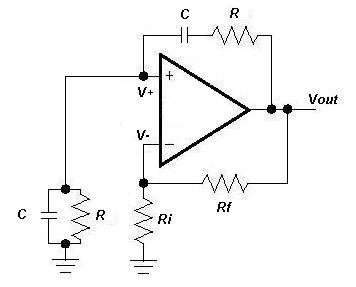
Figure 3
Firstly, from Equation 3 the voltage at the inverting pin is
It is worth noting that if two admittances are placed in series, the total admittance is the inverse of the sum of their reciprocals (using the same formula as for two resistors in parallel). Similarly if two admittances are placed in parallel, the total admittance is sum of the admittances. Therefore the admittance from the output of the op amp to the non inverting input is
Likewise the admittance from the non inverting terminal to ground is
Using the methodology from before, it can be shown that (eventually)
Putting s=jw and
gives
Therefore, using the principles of nodal analysis, the transfer function for the Wien bridge oscillator has been derived. From this equation two conclusions can be drawn, both of which are well known conditions for oscillation of the Wien bridge oscillator.
Firstly, for oscillation to occur there must be zero phase shift from the input to the output. This only happens at one frequency (when
At this frequency the real terms of the numerator cancel and the phase shift represented by the imaginary terms in both numerator and denominator cancel (essentially, if there are no j terms in either numerator or denominator, there is no phase shift). Secondly, at this frequency the ratio of Vout to V+ (hence V-) has to be 3. Anything less than 3 and the oscillation will decay. Anything greater than 3 and the output will saturate. This dictates the ratio of Gf to Gi to maintain oscillation. Rf must be equal to precisely twice the value of Ri.
Conclusions
Using Kirchoff’s law the currents flowing into and out of the nodes around the op amp can be translated into equations and from this the transfer function can be derived. The above examples use admittances instead of impedances, but the principles are the same and it is left to the engineer to decide which is more suitable. Once the equations have been derived, the maths (depending on the complexity of the circuit) is moderately straight forward to obtain the transfer function. Then the power of maths processing programs can be unleashed on the equations to find when for example instability occurs, or the susceptibility of the circuit to component variations, if this is desired.
LTspice is a registered trademark of Analog Devices Inc
Sitemap: www.simonbramble.co.uk/sitemap
© Copyright Simon Bramble