QPSK Modulation Demystified
This article sets out to explain how phase shift modulation works using high school mathematics (trigonometric identities).
Ever since the turn of the century, people have realised the importance of the need to communicate. Since the early days of electronics, as advances in technology took place, the boundaries of both local and global communication have been eroded, resulting in a world that is smaller and hence more easily accessible for the sharing of knowledge and information. The pioneering work done by Bell and Marconi have formed the cornerstone of the information age that exist today and have paved the way for the future of telecommunications.
Traditionally local communication was done over wires as this presented a cost effective way of ensuring reliable information transfer. For long distance communications, transmission of information over radio waves was needed and although it was convenient from a hardware viewpoint, it raised doubts over the corruption of the information and was often dependent on high power transmitters to overcome weather conditions, large buildings and interference from other sources of electromagnetics.
The various modulation techniques offered different solutions in terms of cost effectiveness and quality of received signal but, until recently were still largely analogue. Frequency modulation and phase modulation presented a certain immunity to noise, whilst amplitude modulation was simpler to demodulate. However more recently since the advent of low cost microcontrollers and the introduction of domestic mobile telephones and satellite communications, digital modulation has gained popularity. With digital modulation techniques come all the advantages that traditional microprocessor circuits have over their analogue counterparts. Any shortfalls in the communications link can be eradicated using software. Information can now be encrypted, error correction can ensure more confidence in received data and the use of DSP can reduce the limited bandwidth allocated to each service.
As with traditional analogue systems, digital modulation can use amplitude, frequency or phase modulation with different advantages. As frequency and phase modulation techniques offer more immunity to noise, they are the preferred scheme for the majority of services in use today and will be discussed in detail below.
Digital Frequency Modulation
A simple variation from traditional analogue frequency modulation (FM) can be implemented by applying a digital signal to the modulation input. Thus the output takes the form of a sinewave at two distinct frequencies. To demodulate this waveform, it is a simple matter of passing the signal through two filters and translating the resultant back into logic levels. Traditionally, this form of modulation has been called Frequency Shift Keying (FSK)
Digital Phase Modulation
Spectrally, Digital Phase Modulation (or Phase Shift Keying - PSK) is very similar to Frequency Modulation. It involves changing the phase of the transmitted waveform instead of the frequency, these finite phase changes representing digital data. In its simplest form, a phase modulated waveform can be generated by using the digital data to switch between two signals of equal frequency but opposing phase. If the resultant waveform is multiplied by a sinewave of equal frequency, two components are generated: one cosine waveform of double the received frequency and one frequency independent term, whose amplitude is proportional to the cosine of the phase shift. Thus filtering out the higher frequency term yields the original modulating data prior to transmission. Although, conceptually, this is difficult to picture, the mathematical proof of the above will be shown later.
Quadrature Phase Shift Modulation
Taking the above concept of PSK one stage further, it can be supposed that the number of phase shifts is not limited to only two states. The transmitted “carrier” can undergo any number of phase changes and by multiplying the received signal by a sinewave of equal frequency will demodulate the phase shifts into frequency independent voltage levels.
This is indeed the case in Quadrature Phase Shift Keying (QPSK). With QPSK, the carrier undergoes four changes in phase and can thus represent four binary bits of data. While this may seem insignificant at first glance, a modulation scheme has now been supposed that enables a carrier to transmit four bits of information instead of two, thus effectively doubling the bandwidth of carrier.
The proof of how phase modulation, and hence QPSK, is demodulated is shown below.
The proof begins by defining Euler’s relation, from whence all the trigonometric identities can be derived (if only I had known this in high school)
Euler’s Relation states:
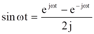
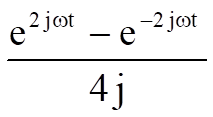
Now consider multiplying two sinewaves together, thus
 =
= 
=
 Equation 1
 From Equation 1, it can be seen that multiplying two sine waves together (one sine being the incoming signal, one being the local oscillator at the receiver mixer), results in an output frequency 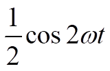 double that of the input (at half the amplitude) superimposed on a dc offset of half the input amplitude.
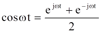
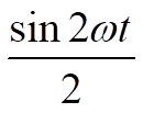
Similarly, multiplying by
by  gives
gives
double that of the input (at half the amplitude) superimposed on a dc offset of half the input amplitude.Similarly, multiplying
= 
which gives an output frequency (
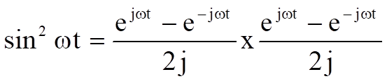
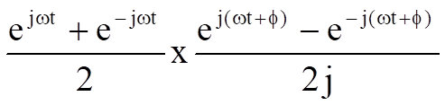
It is now fair to make the assumption that multiplying
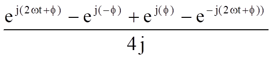
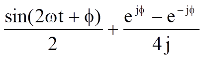
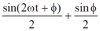
To prove this,
 =
= 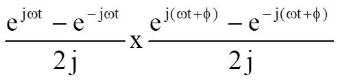
=
=
=
=
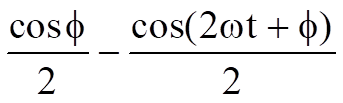
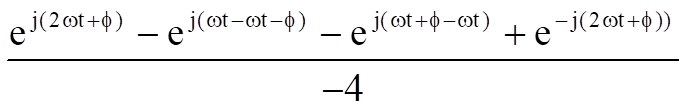
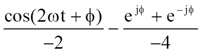
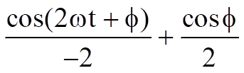
Thus the above proves the supposition that the phase shift on a carrier can be demodulated into a varying output voltage by multiplying the carrier with a sinewave local oscillator and filtering out the high frequency term. Unfortunately, the phase shift is limited to two quadrants - a phase shift of 45 degrees cannot be distinguished from a phase shift of 315 degrees (360 degrees – 45 degrees) Therefore, to accurately decode phase shifts present in all four quadrants, the input signal needs to be multiplied by both sinusoidal and cosinusoidal waveforms, the high frequency filtered out and the data reconstructed. The proof of this, expanding on the above mathematics, is shown below.
Thus,
= 
=
=
=
An LTspice® simulation verifies the above theory.
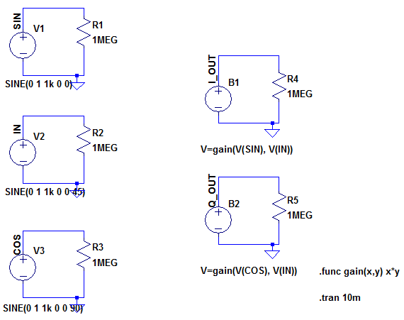
Figure 1
The circuit can be downloaded here: LTspice simulation of QPSK Modulation
Figure 1 shows an LT Spice simulation of a simple demodulator circuit. V2 is the incoming signal (that is going to undergo a phase shift) and V1 and V3 are the sine and cosine local oscillators respectively.
B1 and B2 are the LTspice way of doing a voltage multiplication. B1 is an arbitrary voltage source whose output is the value V(SIN) x V(IN), so the voltage across R4 is the resultant output when these two voltages have been multiplied together. B2 is the same, but the resultant output is the multiplication of V(COS) and V(IN).
All voltages are 1V amplitude at 1kHz, centred about 0V.
With no phase shift on VIN, the I and Q outputs are shown in Figure 2:
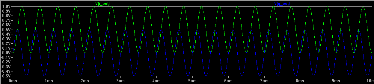
Figure 2
We can see that the I_Out waveform is as expected when two sinewaves are multiplied together – we get a cosine output of half the amplitude but twice the frequency (2kHz) on a dc offset equal to
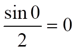
For a phase shift of 0 degrees on the input oscillator, this equates to an offset of
Looking at Q_Out, this is the result of multiplying a sine (with 0 phase shift) by a cosine. We have a waveform with twice the frequency, half the amplitude and a dc offset equal to
If we apply a phase shift to the input of 90 degrees, we get the output shown in Figure 3:
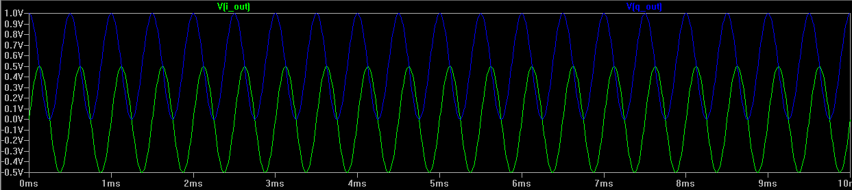
Figure 3
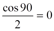
Here we see that I_Out has undergone a dc shift equal to
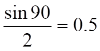
And Q_Out has undergone a dc shift equal to
The above steps can be repeated for different phase shifts on VIN to show that the offset voltage of both the I and Q outputs shifts in proportion to the phase shift. It can be shown that if the phase shift is a multiple of 90 degrees, this results in a dc offset voltage of 0.5V between the I and Q channels. As we can have four 90 degree phase shifts in 360 degrees, this allows us to transmit 4 bits over a single carrier, just by phase shifting the carrier.
Thus if the output voltages are low pass filtered and fed into a dual ADC, the receiver can pick out the dc offset and demodulate the data.
The above theory is perfectly acceptable and it would appear that removing the data from the carrier is a simple process of low pass filtering the output of the mixer and reconstructing the four voltages back into logic levels. In practice, getting a receiver local oscillator exactly synchronised with the incoming signal is not easy. If the local oscillator varies in phase with respect to the incoming signal, the dc offset will change, its magnitude equal to the phase difference.
Therefore, it is not a simple matter of detecting the dc offsets with comparators. A bit more intelligence is needed.
Linear Technology's range of RF products and high speed low power data converters are ideally suited to perform such demodulation tasks.
This article is published on the Analog Devices website: QPSK Modulation Demystified
LTspice is a registered trademark of Analog Devices Inc
Sitemap: www.simonbramble.co.uk/sitemap
© Copyright Simon Bramble